
Page 61 - Embedded Microprocessor Systems Real World Design
P. 61
ADDRESS
DECODING
LOGIC
I :ELECT
ADDR 835
MICROPROCESSOR
IC
ADDRESS ADDRESS
-
LATCH INPUTS
ADDR 0:7
ADDRESSDATA < > I c
MULTIPLEXED
BUS
8 BITS DEHULTIPLWD
- ADDRESS OUTPUT
BUS ENABLE
-RD - * WRITE
-WR r ENABLE
DATA BUS
’ TO OTHER MEMORY
’ AND PERIPHERALS
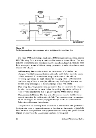
Figure 2.7
RAM Connected to a Microprocessor with a Multiplexed Address/Data Bus.
For static RAM and during a read cycle, RAM timing is calculated the same as
EPROM timing. For a write cycle, additional factors must be considered. First, the
data and control setup and hold times must be calculated. Figure 2.8 shows a static
RAM write cycle. Several additional timing parameters must be taken into consid-
eration with a RAM:
Address setup time. Unlike an EPROM, the contents of a RAM can be
changed. The RAM requires that the address be stable before the write strobe
(-WR) is asserted. If the minimum setup time is not met, the address
decoding logic inside the RAM still may be changing when -WR is asserted,
and the wrong address or multiple addresses may be changed. Note that the
address setup time applies to the leading edge of the -WR strobe.
Data setup time. To guarantee that the correct data are written to the selected
location, the data must be stable before the trailing edge of the -WR signal.
This provides time for the data to get through the RAM’s internal delays.
Data/address hold times. The data and address must each be held for some
specific time after the trailing edge of -WR. This guarantees that the negation
of the -WR signal has time to propagate through the RAM’s internal delays
before the address and data change.
The price for not meeting these parameters is intermittent RAM problems-
locations that seem to change at random or data that are incorrectly written. Like
EPROM access time problems, the symptoms may occur only with specific brands
of parts or only when the temperature reaches a certain point.
46 Embedded Macr@rocessm Systems