
Page 58 - Embedded Microprocessor Systems Real World Design
P. 58
TMSlSMEACCESSllMETHE I
ANY DELAYS IN THE ADDRESS PATH MVtCE MUST HAM To MEET
(SUCH AS ME MMlEsS LATCH)
WILL PUSH THIS LINE TO THE I ACCESSTIME. I ANY DELAYS IN THE DATA PATH
RlW BY THE AMOUNT OF THE (SUCH AS DATA EUS BUFFER)
DELAY. WILL PVSH TMS LINE To TM
THIS IS TM MICROPROCESSOR LEFT BY THE AUWNT OF THE
ACCESS TIME. DELAY.
CLOCK
I I I
I
ALE
I I I
I I I I
DATA BUS ADDR >
. .
, I I I
-RD I I
I I
I I
I I
YTN 4 ~ T W
I I
ADDRESS TO DMCE ADDR
AFTER ADDRESS
LATCH
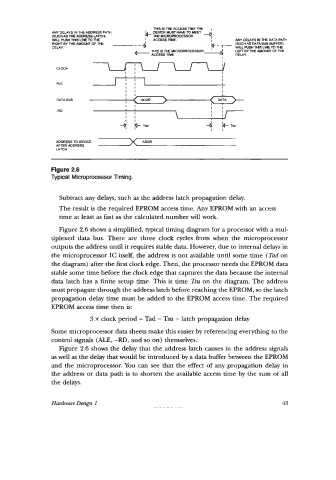
Figure 2.6
Typical Microprocessor Timing.
Subtract any delays, such as the address latch propagation delay.
The result is the required EPROM access time. Any EPROM with an access
time at least as fast as the calculated number will work.
Figure 2.6 shows a simplified, typical timing diagram for a processor with a mul-
tiplexed data bus. There are three clock cycles from when the microprocessor
outputs the address until it requires stable data. However, due to internal delays in
the microprocessor IC itself, the address is not available until some time (Tad on
the diagram) after the first clock edge. Then, the processor needs the EPROM data
stable some time before the clock edge that captures the data because the internal
data latch has a finite setup time. This is time Tsu on the diagram. The address
must propagate through the address latch before reaching the EPROM, so the latch
propagation delay time must be added to the EPROM access time. The required
EPROM access time then is:
3 x clock period - Tad - Tsu - latch propagation delay
Some microprocessor data sheets make this easier by referencing everything to the
control signals (ALE, -RD, and so on) themselves.
Figure 2.6 shows the delay that the address latch causes in the address signals
as well as the delay that would be introduced by a data buffer between the EPROM
and the microprocessor. You can see that the effect of any propagation delay in
the address or data path is to shorten the available access time by the sum of all
the delays.
Hardware Design I 43