
Page 62 - Embedded Microprocessor Systems Real World Design
P. 62
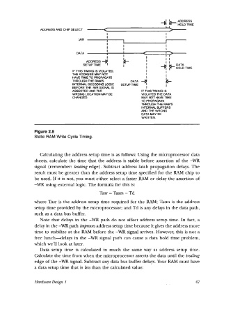
ADDRESS
                                                                         ..   HOLD TIME
                  ADDRESS AND CHIP SELECT
                                               I                         I
                                               I                         I
                                   -WR                                   I
                                              1
                                                                         I
                                                      I
                                               I
                                                       I
                                                                         I
                                  DATA  I(
                                                                         1
                                                                         1
                                               I      !         I        ..
                                      ADDRESS
                                     SETLIPTIME   I
                                IF THIS TIMING IS VIOLATED.
                                THE ADDRESS MAY NOT             I        I
                                HAVE TIME TO PROPAGATE          I
                                THROUGH THE RAM'S         DATA           k-
                                INTERNAL DECODING LOGIC   SETUPTIME   I   I
                                BEFORE THE -WR SIGNAL IS        I
                                ASSERTEDANDTHE                IF THIS TIMING IS
                                WRONG LOCATION MAY BE         VlOLAlED THE DATA
                                CHANGED.                      MAY NOT HAVE TIME
                                                              TO PROPAGATE
                                                              THROUGH ME RAM'S
                                                              INTERNAL BUFFERS
                                                              AND THE WRONG
                                                              DATA MAY BE
                                                              WRITEN.
                Figure 2.8
                Static RAM Write Cycle Timing.
                  Calculating the address setup time is as follows: Using the microprocessor data
                sheets, calculate the time  that the  address is stable before  assertion of the -WR
                signal  (remember:  leuding edge). Subtract address latch propagation  delays. The
                result must be greater than the address setup time specified for the RAM chip to
                be used. If it is not, you must either select a faster RAM or delay the assertion of
                -WR  using external logic. The formula for this is:
                                            Tasr = Tasm - Td

                where Tasr is the address setup time required for the RAM; Tasm is the address
                setup time provided by the microprocessor; and Td is any delays in the data path,
                such as a data bus buffer.
                  Note that delays in  the -WR  path  do not affect address setup time. In fact, a
                delay in the -WR  path impoves address setup time because it gives the address more
                time to stabilize at the RAM before the -WR  signal arrives. However, this is not a
                free lunch-delays in  the -wR  signal path  can cause a data hold  time problem,
                which we'll look at later.
                  Data  setup  time  is  calculated  in  much  the  same way  as  address  setup  time.
                Calculate the time from when the microprocessor asserts the data until the trailing
                edge of the -WR  signal. Subtract any data bus buffer delays. Your RAM must have
                a data setup time that is less than the calculated value:


                Hardware Design 1                                                     47