
Page 64 - Embedded Microprocessor Systems Real World Design
P. 64
DATA STROBE READ STROBE
READSTROBE - WRITE STROBE
(O=ACTIM)
(O=ACTIM)
DIRECTION
(5WRITE)
(O=ACTIM)
I
DATA STROBE
DIRECTION
WRITE STROBE 1 /
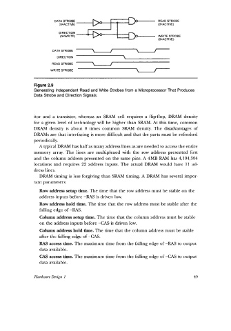
Figure 2.9
Generating Independent Read and Write Strobes from a Microprocessor That Produces
Data Strobe and Direction Signals.
itor and a transistor, whereas an SRAM cell requires a flip-flop, DRAM density
for a given level of technology will be higher than SRAM. At this time, common
DRAM density is about 8 times common SRAM density. The disadvantages of
DRAMS are that interfacing is more difficult and that the parts must be refreshed
periodically.
A typical DRAM has half as many address lines as are needed to access the entire
memory array. The lines are multiplexed with the row address presented first
and the column address presented on the same pins. A 4MB RAM has 4,194,304
locations and requires 22 address inputs. The actual DRAM would have 11 ad-
dress lines.
DRAM timing is less forgiving than SRAM timing. A DRAM has several impor-
tant parameters:
Row address setup time. The time that the row address must be stable on the
address inputs before -RAS is driven low.
Row address hold time. The time that the row address must be stable after the
falling edge of -RAS.
Column address setup time. The time that the column address must be stable
on the address inputs before -CAS is driven low.
Column address hold time. The time that the column address must be stable
after the falling edge of -CAS.
RAS access time. The maximum time from the falling edge of -RAS to output
data available.
CAS access time. The maximum time from the falling edge of -CAS to output
data available.
Hardware Design I 49