
Page 231 - Academic Press Encyclopedia of Physical Science and Technology 3rd Polymer
P. 231
P1: GOJ/GOI/LCC/HAR P2: GOJ Final Pages
Encyclopedia of Physical Science and Technology en012K-946 July 26, 2001 11:14
740 Polymers, Photoresponsive
and use of such resists in full-scale semiconductor man-
ufacturing, in spite of superior process latitude, mainly
because of the dependence of resist performance on a set
of new process variables such as the time elapsed between
exposure to post-exposure bake, basic contaminants in the
clean room, and substrate and the amount of protecting
groups on the polymer.
Basic mechanistic understanding of the molecular
structure and interactions of resist components (polymer,
photoacid generator, base additive, protecting groups) as
they relate to process performance have led to robust resist
design.Itisnoexaggerationtosaythatsuchrobustyetvery
high-resolution resist materials are responsible to a large
extent for the extension of optical lithography capabili-
ties to fabricate devices of design rules that are roughly
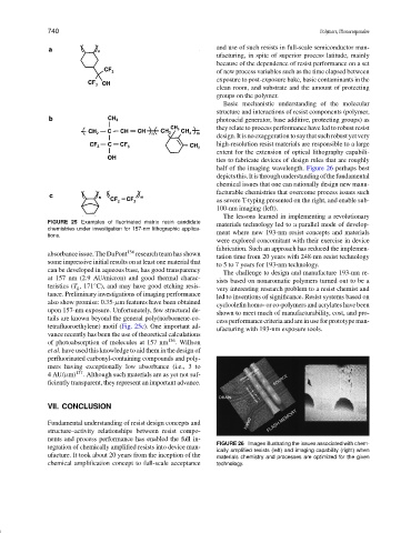
half of the imaging wavelength. Figure 26 perhaps best
depictsthis.Itisthroughunderstandingofthefundamental
chemical issues that one can rationally design new manu-
facturable chemistries that overcome process issues such
as severe T-typing presented on the right, and enable sub-
100-nm imaging (left).
The lessons learned in implementing a revolutionary
FIGURE 25 Examples of fluorinated matrix resin candidate
materials technology led to a parallel mode of develop-
chemistries under investigation for 157-nm lithographic applica-
ment where new 193-nm resist concepts and materials
tions.
were explored concomitant with their exercise in device
fabrication. Such an approach has reduced the implemen-
absorbance issue. The DuPont 134 research team has shown
tation time from 20 years with 248-nm resist technology
some impressive initial results on at least one material that
to 5 to 7 years for 193-nm technology.
can be developed in aqueous base, has good transparency
The challenge to design and manufacture 193-nm re-
at 157 nm (2.9 AU/micron) and good thermal charac-
sists based on nonaromatic polymers turned out to be a
◦
teristics (T g , 171 C), and may have good etching resis-
very interesting research problem to a resist chemist and
tance. Preliminary investigations of imaging performance
led to inventions of significance. Resist systems based on
also show promise: 0.35-µm features have been obtained
cycloolefin homo- or co-polymers and acrylates have been
upon 157-nm exposure. Unfortunately, few structural de-
shown to meet much of manufacturability, cost, and pro-
tails are known beyond the general poly(norbornene-co-
cess performance criteria and are in use for prototype man-
tetrafluoroethylene) motif (Fig. 25c). One important ad-
ufacturing with 193-nm exposure tools.
vance recently has been the use of theoretical calculations
of photoabsorption of molecules at 157 nm 136 . Willson
et al. have used this knowledge to aid them in the design of
perfluorinated carbonyl-containing compounds and poly-
mers having exceptionally low absorbance (i.e., 3 to
4AU/µm) 137 . Although such materials are as yet not suf-
ficiently transparent, they represent an important advance.
VII. CONCLUSION
Fundamental understanding of resist design concepts and
structure–activity relationships between resist compo-
nents and process performance has enabled the full in-
FIGURE 26 Images illustrating the issues associated with chem-
tegration of chemically amplified resists into device man-
ically amplified resists (left) and imaging capability (right) when
ufacture. It took about 20 years from the inception of the materials chemistry and processes are optimized for the given
chemical amplification concept to full-scale acceptance technology.