
Page 268 - Engineering Digital Design
P. 268
6.1 INTRODUCTION AND BACKGROUND 239
50%
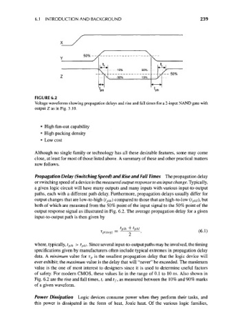
FIGURE 6.2
Voltage waveforms showing propagation delays and rise and fall times for a 2-input NAND gate with
output Z as in Fig. 3.10.
• High fan-out capability
• High packing density
• Low cost
Although no single family or technology has all these desirable features, some may come
close, at least for most of those listed above. A summary of these and other practical matters
now follows.
Propagation Delay (Switching Speed) and Rise and Fall Times The propagation delay
or switching speed of a device is the measured output response to an input change. Typically,
a given logic circuit will have many outputs and many inputs with various input-to-output
paths, each with a different path delay. Furthermore, propagation delays usually differ for
output changes that are low-to-high (t pih) compared to those that are high-to-low (t phi\ but
both of which are measured from the 50% point of the input signal to the 50% point of the
output response signal as illustrated in Fig. 6.2. The average propagation delay for a given
input-to-output path is then given by
where, typically, t pih > t pM . Since several input-to-output paths may be involved, the timing
specifications given by manufacturers often include typical extremes in propagation delay
data. A minimum value for r p is the smallest propagation delay that the logic device will
ever exhibit; the maximum value is the delay that will "never" be exceeded. The maximum
value is the one of most interest to designers since it is used to determine useful factors
of safety. For modern CMOS, these values lie in the range of 0.1 to 10 ns. Also shown in
Fig. 6.2 are the rise and fall times, t r and tf, as measured between the 10% and 90% marks
of a given waveform.
Power Dissipation Logic devices consume power when they perform their tasks, and
this power is dissipated in the form of heat, Joule heat. Of the various logic families,