Page 273 - Engineering Digital Design
P. 273

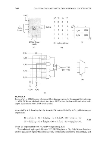
244               CHAPTER 6 / NONARITHMETIC COMBINATIONAL LOGIC DEVICES


                           EN(L)
                                                        EN S, 1  S n 0  Y
                                                        0  X   X    0

                                                        1   0  0           0
                                                Output              'o  S^v   0      1
                                                        1   0  1    '1   °   V EN   I^N

                                                        1   1  0
                                                                    '2   1   I 2EEN  I 3EN
                                                        1   1   1   '3                  /
                                2 Data Select          X = Irrelevant Input      (c)
                                   Inputs

                                    (a)                       (b)


                                                                              — c\

                                                                    Y(H)      —
                                                                    Y(L)      —


                           I 3(H)                _
                                                                                ^
                                                                                  (e)


                                S,(H)  S 0(H)
                                               (d)
                    FIGURE 6.4
                    Design of a 4-to-l MUX or data selector, (a) Block diagram symbol, (b) Compressed EV truth table.
                    (c) MUX EV K-map. (d) Logic circuit for a 4-to-l MUX with active low enable and mixed logic
                    output, (e) Shorthand 4-to-l MUX circuit symbol.


                    shown in Fig. 6.6. Reading directly from the EV truth table in Fig. 6.6a yields the output
                    expressions

                             17= SiSol/o- IG + SiSolIi • lG + SiSol/2 • IG + S 1S 0II 3 • 1G
                                                                                        (6.6)
                             27 = SiS 02I 0 • 2G + SiS Q2Ii • 2G + S }S 02I 2 • 2G + 5i5 02/ 3 • 2G,

                    which are implemented with NAND/INV logic in Fig. 6.6c.
                       The traditional logic symbol for the '153 MUX is given in Fig. 6.6b. Notice that there
                    are two data select inputs that simultaneously control data selection to both outputs, and
   268   269   270   271   272   273   274   275   276   277   278