
Page 272 - Engineering Digital Design
P. 272
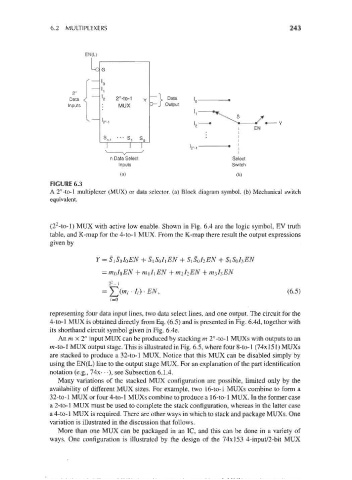
6.2 MULTIPLEXERS                                                    243


                            EN(L)

                              Lo G
                            f-   0

                        2 , - 1
                                      n
                        Data <J  '2  2 -to-1  Y    Data    |        .
                       Inputs  ]  :  MUX           Output
                            [_                             '  *^\
                                                           1
                                                                    ^^
                                 '2"-!                     I   •
                                                           '2
                                 S
                                  n-1 •" S 1  S Q
                                   n Data Select
                                     Inputs
                                      (a)                              (b)
                  FIGURE 6.3
                     !
                 A 2' -to-l multiplexer (MUX) or data selector, (a) Block diagram symbol, (b) Mechanical switch
                 equivalent.


                   2
                  (2 -to-l) MUX with active low enable. Shown in Fig. 6.4 are the logic symbol, EV truth
                 table, and K-map for the 4-to-l MUX. From the K-map there result the output expressions
                 given by

                               Y = SiS 0I 0EN + SiS QIiEN + S {S QI 2EN
                                = m 0I 0EN + mil\ EN


                                     (m, - /,-) • EN,                                 (6.5)
                                   i=0

                 representing four data input lines, two data select lines, and one output. The circuit for the
                 4-to-l MUX is obtained directly from Eq. (6.5) and is presented in Fig. 6.4d, together with
                 its shorthand circuit symbol given in Fig. 6.4e.
                    An m x 2" input MUX can be produced by stacking m 2"-to-l MUXs with outputs to an
                 m-to-1 MUX output stage. This is illustrated in Fig. 6.5, where four 8-to-l (74x151) MUXs
                 are stacked to produce a 32-to-l MUX. Notice that this MUX can be disabled simply by
                 using the EN(L) line to the output stage MUX. For an explanation of the part identification
                 notation (e.g., 74x- • •), see Subsection 6.1.4.
                    Many variations of the stacked MUX configuration are possible, limited only by the
                 availability of different MUX sizes. For example, two 16-to-l MUXs combine to form a
                 32-to-l MUX or four 4-to-l MUXs combine to produce a 16-to-l MUX. In the former case
                 a 2-to-l MUX must be used to complete the stack configuration, whereas in the latter case
                 a 4-to-l MUX is required. There are other ways in which to stack and package MUXs. One
                 variation is illustrated in the discussion that follows.
                    More than one MUX can be packaged in an 1C, and this can be done in a variety of
                 ways. One configuration is illustrated by the design of the 74x153 4-input/2-bit MUX