
Page 288 - Engineering Digital Design
P. 288
6.5 CODE CONVERTERS 259
C+D C+D
BCD XS3
1
A B c D A B' C' D 1 C+D
0 0 0 0 0 0 1 1
0 0 0 1 0 1 0 0
0 0 1 0 0 1 0 1
0 0 1 1 0 1 1 0
0 1 0 0 0 1 1 1
0 1 0 1 1 0 0 0
0 1 1 0 1 0 0 1
0 1 1 1 1 0 1 0 D 1
1 0 0 0 1 0 1 1
1 0 0 1 1 1 0 0
1 0 1 1 1 L
1 0 1 0
1 1 0 0 s
1 1 0 1 ^
1 1 1 0 B(H)
1 1 1 1 1 BCD;
Inpur XS3
(a)
Output
D(H)-
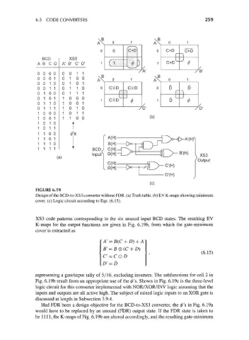
FIGURE 6.19
Design of the BCD-to-XS3 converter without FDR. (a) Truth table, (b) EV K-maps showing minimum
cover, (c) Logic circuit according to Eqs. (6.15).
XS3 code patterns corresponding to the six unused input BCD states. The resulting EV
K-maps for the output functions are given in Fig. 6.19b, from which the gate-minimum
cover is extracted as
A' =
B' = B 0 (C + D)
(6.15)
C' = CQD
D' = D
representing a gate/input tally of 5/10, excluding inverters. The subfunctions for cell 2 in
Fig. 6.19b result from an appropriate use of the 0's. Shown in Fig. 6.19c is the three-level
logic circuit for this converter implemented with NOR/XOR/INV logic assuming that the
inputs and outputs are all active high. The subject of mixed logic inputs to an XOR gate is
discussed at length in Subsection 3.9.4.
Had FDR been a design objective for the BCD-to-XS3 converter, the 0's in Fig. 6.19a
would have to be replaced by an unused (FDR) output state. If the FDR state is taken to
be 1111, the K-maps of Fig. 6.19b are altered accordingly, and the resulting gate-minimum