
Page 431 - Hacking Roomba
P. 431
412 Appendix B — Electrical Diagram Schematics
Integrated Circuits and Other Complex Components
When electrical components were being created and discovered, it seemed appropriate to
draw specialized symbols for each one. As individual components became more complex inter-
nally, it became harder to describe symbolically what a component did. The most complex
devices came to be represented as simple boxes. An intermediary form is the relay above: a
compound device with a box drawn around it to show it’s a single unit. The internals of that
box don’t need to be shown as long as the terminals exiting are labeled appropriately. It will
still be understood to be a relay.
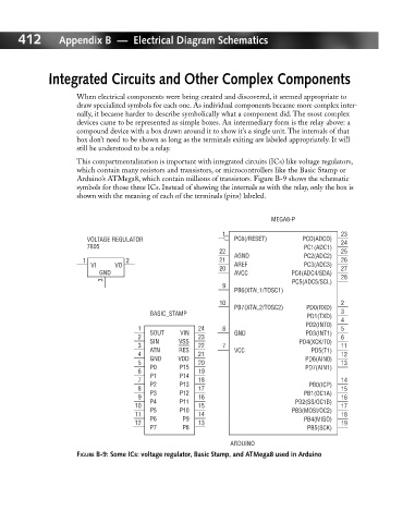
This compartmentalization is important with integrated circuits (ICs) like voltage regulators,
which contain many resistors and transistors, or microcontrollers like the Basic Stamp or
Arduino’s ATMega8, which contain millions of transistors. Figure B-9 shows the schematic
symbols for those three ICs. Instead of showing the internals as with the relay, only the box is
shown with the meaning of each of the terminals (pins) labeled.
MEGA8-P
1 23
VOLTAGE REGULATOR PC6(/RESET) PCO(ADCO)
7805 PC1(ADC1) 24
22 25
AGND PC2(ADC2)
1 2 21 26
VI VO 20 AREF PC3(ADC3) 27
GND AVCC PC4(ADC4/SDA)
3 PC5(ADC5/SCL) 28
9
PB6(XTAL1/TOSC1)
10 2
PB7(XTAL2/TOSC2) PD0(RXD)
BASIC_STAMP 3
PD1(TXD)
4
PD2(INT0)
1 24 8 5
SOUT VIN GND PD3(INT1)
2 23 6
SIN VSS PD4(XCK/T0)
3 22 7 11
ATN RES VCC PD5(T1)
4 21 12
GND VDD PD6(AIN0)
5 20 13
P0 P15 PD7(AIN1)
6 19
P1 P14
7 18 14
P2 P13 PB0(ICP)
8 17 15
P3 P12 PB1(OC1A)
9 16 16
P4 P11 PB2(SS/OC1B)
10 15 17
P5 P10 PB3(MOSI/OC2)
11 14 18
P6 P9 PB4(MISO)
12 13 19
P7 P8 PB5(SCK)
ARDUINO
FIGURE B-9: Some ICs: voltage regulator, Basic Stamp, and ATMega8 used in Arduino