
Page 66 - High Power Laser Handbook
P. 66
38 G a s , C h e m i c a l , a n d F r e e - E l e c t r o n L a s e r s Excimer Lasers 39
2.4.2 Brighter Displays
Over the past 10 years, the global flat panel display industry has shown
tremendous growth in all display segments, from small mobile phones
and car navigation displays to large home entertainment and advertis-
ing panels. Emerging display technologies, such as organic light-emitting
diodes (OLEDs) or displays based on flexible substrates, will further
drive the industry’s rapid growth. In recent years, low-temperature
polycrystalline silicon (LTPS) has demonstrated its advantages through
successful implementation in applications such as highly integrated
active-matrix liquid crystal displays (AMLCDs) and, most recently,
active-matrix organic light-emitting diode displays (AMOLEDs).
Advances in manufacturing equipment have enabled the display
industry to take advantage of larger glass sizes and improved econo-
mies of scale. For LTPS, this progress is manifested in the excimer laser
source—in particular, output power, shot noise, and the optical beam
delivery system that delivers the light to the substrate for the controlled
14
crystallization process. The annealing process demands tight control
of every single laser pulse, making pulse-to-pulse (p2p) energy stabil-
ity an extremely important laser parameter. Advances in this area over
the past few years have substantially increased the available energy,
thus satisfying the increasing demand for higher yields on larger glass
plates and the demand for LTPS backplanes for AMOLED. The exci-
mer laser process transforms the low-electron mobility silicon into an
enabling thin film of 50-nm thickness, which supports fast voltage
switching of the thin film transistor (TFT) for high-resolution AMLCDs,
as well as the required current driving of emerging AMOLEDs.
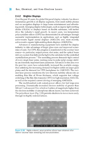
The multihundred-watt output power allows for fast large-area
processing. Dramatically increased electron mobility of greater than
100 cm /volt-second (Vs), which is 2 orders of magnitude higher than
2
the electron mobility of amorphous silicon layers, has been achieved.
The polysilicon layer (Fig. 2.20) permits electrons to move more easily
through its highly ordered lattices.
Figure 2.20 Highly ordered, polycrystalline silicon layer obtained after
308-nm excimer laser annealing and recrystallization.