
Page 63 - High Power Laser Handbook
P. 63
34 G a s , C h e m i c a l , a n d F r e e - E l e c t r o n L a s e r s Excimer Lasers 35
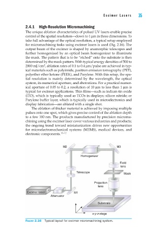
2.4.1 High-Resolution Micromachining
The unique ablation characteristics of pulsed UV lasers enable precise
control of the spatial resolution—down to 1 mm in three dimensions. To
take full advantage of the optical resolution, a typical setup employed
for micromachining tasks using excimer lasers is used (Fig. 2.16). The
output beam of the excimer is shaped by anamorphic telescopes and
further homogenized by an optical beam homogenizer to illuminate
the mask. The pattern that is to be “etched” onto the substrate is then
determined by the mask pattern. With typical energy densities of 500 to
2
2000 mJ/cm , ablation rates of 0.1 to 0.4 mm/pulse are achieved in typ-
ical materials such as polyimide, positron emission tomography (PET),
polyether ether ketone (PEEK), and Parylene. With this setup, the spa-
tial resolution is mainly determined by the wavelength, the optical
system, its numerical aperture, and aberrations. For a practical numer-
ical aperture of 0.05 to 0.2, a resolution of 10 mm to less than 1 mm is
typical for excimer applications. Thin films—such as indium tin oxide
(ITO), which is typically used as TCOs in displays; silicon nitride; or
Parylene buffer layer, which is typically used in microelectronics and
display fabrication—are ablated with a single shot.
The ablation of thicker material is achieved by imposing multiple
pulses onto one spot, which gives precise control of the ablation depth
to a few 100 nm. The products manufactured by precision microma-
chining using the excimer laser cover various industries and products;
the ongoing trend toward miniaturization drives new opportunities
for microelectromechanical systems (MEMS), medical devices, and
electronic components. 10–12
M2 M3
Homogenizer
Field
lens
Telescope
Mask
Projection
lens
Excimer laser M1
Attenuator
Substrate
x-y-z-stage
Figure 2.16 Typical layout for excimer micromachining system.