
Page 65 - High Power Laser Handbook
P. 65
36 G a s , C h e m i c a l , a n d F r e e - E l e c t r o n L a s e r s Excimer Lasers 37
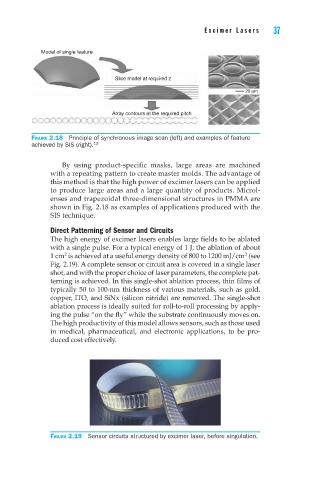
Model of single feature
Slice model at required z
20 µm
Array contours at the required pitch
Figure 2.18 Principle of synchronous image scan (left) and examples of feature
achieved by SIS (right). 13
By using product-specific masks, large areas are machined
with a repeating pattern to create master molds. The advantage of
this method is that the high power of excimer lasers can be applied
to produce large areas and a large quantity of products. Microl-
enses and trapezoidal three-dimensional structures in PMMA are
shown in Fig. 2.18 as examples of applications produced with the
SIS technique.
Direct Patterning of Sensor and Circuits
The high energy of excimer lasers enables large fields to be ablated
with a single pulse. For a typical energy of 1 J, the ablation of about
2
1 cm is achieved at a useful energy density of 800 to 1200 mJ/cm (see
2
Fig. 2.19). A complete sensor or circuit area is covered in a single laser
shot, and with the proper choice of laser parameters, the complete pat-
terning is achieved. In this single-shot ablation process, thin films of
typically 50 to 100-nm thickness of various materials, such as gold,
copper, ITO, and SiNx (silicon nitride) are removed. The single-shot
ablation process is ideally suited for roll-to-roll processing by apply-
ing the pulse “on the fly” while the substrate continuously moves on.
The high productivity of this model allows sensors, such as those used
in medical, pharmaceutical, and electronic applications, to be pro-
duced cost effectively.
Figure 2.19 Sensor circuits structured by excimer laser, before singulation.