
Page 314 - System on Package_ Miniaturization of the Entire System
P. 314
288 Cha pte r F i v e
1.5
1.0
0.5
Capacitance change (%) −0.5 −60 −40 −20 0 20 Pure BCB 60 80 100 120
0.0
40
−1.0
−1.5
20% Ta O
2
30% Ta O
2
−2.0
40% Ta O 5 5 5
2
−2.5
−3.0
Temperature (°C)
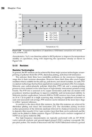
FIGURE 5.24 Temperature dependence of capacitance of BCB-based composites with various
Ta 2 O 5 contents. [55]
characteristics. Ta O was therefore added to BCB polymer to improve the temperature
2
5
stability of capacitance, along with improving the capacitance density as shown in
Figure 5.24.
5.4.6 Resistors
Resistor Technologies
In general, the RF resistors can be achieved by three major process technologies: screen-
printing of polymer thick film (PTF), electroless plating, and direct foil lamination.
The polymer thick films have instability problems in the microwave frequency
range due to their moisture absorption. However, these thick films offer much higher
resistance that is suitable for the pull-up, pull-down, and circuit isolation. As such, PTF
is a mature technology that has been applied into numerous products [56]. For example,
Motorola uses carbon-phenolic polymer thick-film (PTF) ink and a screen-printing
process to form resistors in the inner layers of high-density interconnect printed wiring
boards. The PTF ink is screened on to copper termination pads that are treated with
proprietary interface metallurgy to improve reliability and environmental stability. In
Motorola product applications, between 8000 to 20,000 resistors have been printed on
an 18 in × 24 in panel in a single screening step, resulting in significant economies of
scale and associated cost savings. PTF resistors can be trimmed at the inner-layer stage
to within 1 percent tolerance.
In contrast to the above thick-film resistors, the thin-film resistors are achieved by
electroless plating and direct foil lamination [57]. The electroless plating involves
surface preparation of the dielectric medium followed by chemical treatment in order
to deposit a thin (usually 0.3 to 1 μm) resistive layer that then can be patterned, and the
stubs can be plated to define resistors. Figure 5.25 shows such a resistor comprised of
NiWP on an epoxy dielectric [58].
The high-frequency measurements are typically performed with an HP 8510C
vector network analyzer and ground-signal-ground (GSG) coplanar waveguide 200-
μm-pitch probes. The results of structures with NiP/NiWP fabricated without a ground