
Page 360 - System on Package_ Miniaturization of the Entire System
P. 360
332 Cha pte r S i x
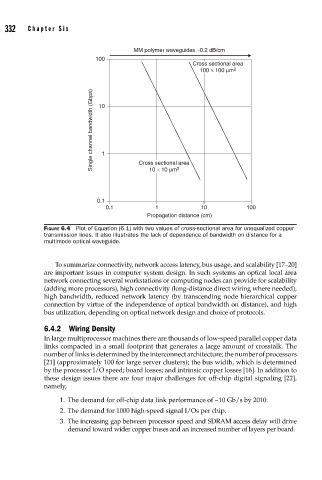
MM polymer waveguides –0.2 dB/cm
100
Cross sectional area
100 × 100 μm 2
Single channel bandwidth (Gbps) 10 1 Cross sectional area
0.1 10 × 10 μm 2
0.1 1 10 100
Propagation distance (cm)
FIGURE 6.4 Plot of Equation (6.1) with two values of cross-sectional area for unequalized copper
transmission lines. It also illustrates the lack of dependence of bandwidth on distance for a
multimode optical waveguide.
To summarize connectivity, network access latency, bus usage, and scalability [17–20]
are important issues in computer system design. In such systems an optical local area
network connecting several workstations or computing nodes can provide for scalability
(adding more processors), high connectivity (long-distance direct wiring where needed),
high bandwidth, reduced network latency (by transcending node hierarchical copper
connection by virtue of the independence of optical bandwidth on distance), and high
bus utilization, depending on optical network design and choice of protocols.
6.4.2 Wiring Density
In large multiprocessor machines there are thousands of low-speed parallel copper data
links compacted in a small footprint that generates a large amount of crosstalk. The
number of links is determined by the interconnect architecture; the number of processors
[21] (approximately 100 for large server clusters); the bus width, which is determined
by the processor I/O speed; board losses; and intrinsic copper losses [16]. In addition to
these design issues there are four major challenges for off-chip digital signaling [22],
namely,
1. The demand for off-chip data link performance of ~10 Gb/s by 2010.
2. The demand for 1000 high-speed signal I/Os per chip.
3. The increasing gap between processor speed and SDRAM access delay will drive
demand toward wider copper buses and an increased number of layers per board.