
Page 72 - MEMS and Microstructures in Aerospace Applications
P. 72
Osiander / MEMS and microstructures in Aerospace applications DK3181_c003 Final Proof page 60 1.9.2005 9:00pm
60 MEMS and Microstructures in Aerospace Applications
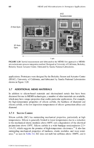
XYZ
Accelerometer
Z-Axis Gyro
XY-Axis
Gyro
1 cm
FIGURE 3.20 Inertial measurement unit fabricated in the MEMS first approach to MEMS-
microelectronics process integration method. Designed at University of California, Berkeley,
Berkeley Sensor Actuator Center. Fabricated by Sandia National Laboratories.
applications. Prototypes were designed by the Berkeley Sensor and Actuator Center
(BSAC), University of California, and fabricated by Sandia National Laboratories
shown in Figure 3.20.
3.7 ADDITIONAL MEMS MATERIALS
In addition to silicon-based materials and electroplated metals that have been
discussed for use in MEMS technologies, a number of other materials are available,
which may have unique properties that enable particular applications. For example,
the high-temperature properties of silicon carbide, the hardness of diamond and
silicon carbide, or the low deposition temperatures of silicon–germanium alloys and
diamond.
3.7.1 SILICON CARBIDE
Silicon carbide (SiC) has outstanding mechanical properties, particularly at high
temperatures. Silicon is generally limited to lower temperatures due to a reduction
in the mechanical elastic modulus above 6008C and a degradation of the electrical
pn-junctions above 1508C. Silicon carbide is a wide bandgap semiconductor (2.3–
3.4 eV), which suggests the promise of high-temperature electronics. 37 It also has
outstanding mechanical properties of hardness, elastic modulus, and wear resist-
ance, 38 as seen in Table 3.6. SiC does not melt but sublimes above 18008C, and it
© 2006 by Taylor & Francis Group, LLC