
Page 73 - MEMS and Microstructures in Aerospace Applications
P. 73
Osiander / MEMS and microstructures in Aerospace applications DK3181_c003 Final Proof page 61 1.9.2005 9:00pm
MEMS Fabrication 61
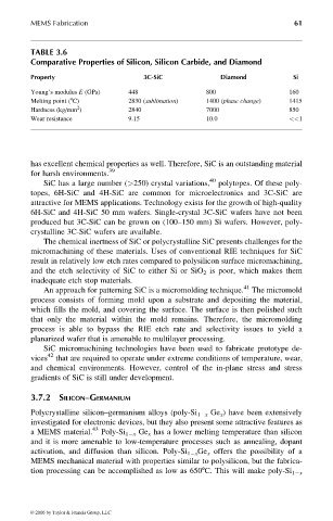
TABLE 3.6
Comparative Properties of Silicon, Silicon Carbide, and Diamond
Property 3C-SiC Diamond Si
Young’s modulus E (GPa) 448 800 160
Melting point (8C) 2830 (sublimation) 1400 (phase change) 1415
2
Hardness (kg/mm ) 2840 7000 850
Wear resistance 9.15 10.0 <<1
has excellent chemical properties as well. Therefore, SiC is an outstanding material
for harsh environments. 39
SiC has a large number (>250) crystal variations, 40 polytopes. Of these poly-
topes, 6H-SiC and 4H-SiC are common for microelectronics and 3C-SiC are
attractive for MEMS applications. Technology exists for the growth of high-quality
6H-SiC and 4H-SiC 50 mm wafers. Single-crystal 3C-SiC wafers have not been
produced but 3C-SiC can be grown on (100–150 mm) Si wafers. However, poly-
crystalline 3C-SiC wafers are available.
The chemical inertness of SiC or polycrystalline SiC presents challenges for the
micromachining of these materials. Uses of conventional RIE techniques for SiC
result in relatively low etch rates compared to polysilicon surface micromachining,
and the etch selectivity of SiC to either Si or SiO 2 is poor, which makes them
inadequate etch stop materials.
41
An approach for patterning SiC is a micromolding technique. The micromold
process consists of forming mold upon a substrate and depositing the material,
which fills the mold, and covering the surface. The surface is then polished such
that only the material within the mold remains. Therefore, the micromolding
process is able to bypass the RIE etch rate and selectivity issues to yield a
planarized wafer that is amenable to multilayer processing.
SiC micromachining technologies have been used to fabricate prototype de-
vices 42 that are required to operate under extreme conditions of temperature, wear,
and chemical environments. However, control of the in-plane stress and stress
gradients of SiC is still under development.
3.7.2 SILICON–GERMANIUM
Polycrystalline silicon–germanium alloys (poly-Si 1 x Ge x ) have been extensively
investigated for electronic devices, but they also present some attractive features as
a MEMS material. 43 Poly-Si 1 x Ge x has a lower melting temperature than silicon
and it is more amenable to low-temperature processes such as annealing, dopant
activation, and diffusion than silicon. Poly-Si 1 x Ge x offers the possibility of a
MEMS mechanical material with properties similar to polysilicon, but the fabrica-
tion processing can be accomplished as low as 6508C. This will make poly-Si 1 x
© 2006 by Taylor & Francis Group, LLC