
Page 439 -
P. 439
7-28 MEMS: Design and Fabrication
package-induced stress and contact degradation, must be resolved. To be commercially viable, these sen-
sors must undergo appropriate reliability testing standards that are specific for harsh-environment
microsystems. However, the existing Joint Electron Device Engineering Council standards are only appli-
cable to conventional-environment semiconductor microsystems [JEDEC Standards]. Because of the
absence of a testing standard for high temperature devices, we recently developed and employed an
Accelerated Stress Test (AST) protocol to evaluate the reliability performance of packaged SiC pressure trans-
ducers up to 300°C in air for over 140 hours under cyclic pressure and temperature [Savrun et al., 2004].
7.6.1 Reliability by Package Design
2
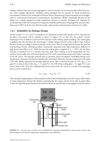
The SiC sensor (2.1 2.1mm ) is mounted on an aluminum nitride (AlN) header (0.25 in. diameter) by
the direct chip attach (DCA) method, as shown in Figure 7.21, so that only the sensor’s circular
diaphragm is free to deflect in and out of the reference cavity [Okojie, patent pending]. The sealing glass
is applied only into and above the narrow gap ( 10 µm) between the SiC sensor and the inner walls of
the AlN, thereby providing a reference pressure in the cavity. This DCA approach eliminates the need for
wire-bonding, thereby eliminating failure mechanisms associated with high-temperature diffusion of
gold bond wires [Khan et al., 1994]. Because the sealing glass is applied at T 750°C, the SiC/glass
δ
interface is assumed to be in a relaxed, stress-free state. Upon cooling to room temperature, the mis-
matches in the coefficients of thermal expansion (CTE) of the contracting components induce a net stress
on the SiC sensor. This package-induced stress is a primary cause of transducer instabilities during cyclic
temperature excursions and must be significantly minimized. Therefore, having components with equal
CTEs will, ideally, eliminate the package-induced stress. AlN is selected because its CTE (α 4.1
AlN
ppm/°C) is close to that of SiC (α 3.7 ppm/°C). The CTE of the sealing glass ( 4.1 ppm/°C) is also
SiC
close to that of SiC. Thus, the resulting induced net strain on the SiC sensor as a result of the packaging
process can be estimated as:
ε (α α )(T T) (7.29)
δ glass SiC δ
This calculation approximates a lateral residual strain of about 300µstrains on the SiC sensor solid surface
at room temperature. Because the distance separating the SiC sensor and the kovar tube is greater than
12mm, the large thermomechanical stress between the kovar and AlN does not propagate to the SiC sensor.
Glass sealed Sensor
gap
AIN
Reference
cavity
Thermocouple
hole
Kovar tube
Contact wire
FIGURE 7.21 Top and cross-sectional views of MEMS-DCA package featuring direct wire contact to sensor and
thermocouple access hole for temperature compensation, and calibration.
© 2006 by Taylor & Francis Group, LLC