
Page 507 -
P. 507
9-28 MEMS: Design and Fabrication
−30
−20 V :
Source-drain current (µA) −150 0 0 −4 −8 −100 V
−10
g
−80 V
−100
−60 V
−50
−40 V
0 −20 V
0 −20 −40 −60 −80 −100
Source-drain voltage (V)
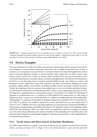
FIGURE 9.26 Transistor characteristic for a microfluidic transitor as shown in Figure 9.10, The mercury extends
completely through the transistor region in this device and the gate length is 110µm and the gate width 2.5 cm. The
inset shows the device characteristics in the linear region (after Maltezos et al. (2003)).
9.4 Device Examples
The mass production of small, low-profile, smart-polymer microsystems enables polymer-based chemi-
cal, biological, or environmental monitoring systems that can be readily incorporated into a variety of
products. Low-cost polymer mass production is extremely attractive for biomedical applications, such as
quick turnaround laboratory analysis or remote medicine, often termed lab-on-a-chip or micro-total-
analysis systems (µTAS). For a review, see Rossier (2002). Similarly, these uses may be extended to envi-
ronmental monitoring for consumer, military, and industrial applications. Demand for this technology is
driven by an ever-increasing need to monitor potential health hazards, toxic threats in warfare, and
homeland security. Applications range from industrial and office environments, shipping and trans-
portation systems, military environments (including wearable systems), and home consumer products.
Clearly, the technology driver for success in these applications is a low-cost, flexible, and robust technol-
ogy that polymer systems have considerable potential to meet. In many applications, polymers are read-
ily employed as sacrificial layers in a microsystem process [Courcimault et al., 2004]. The advantages of
polymers as sacrificial layers are: (1) a polymer is readily applied at low temperatures at a wide range of
thicknesses, from 1 µmtotens of microns thick; (2) a polymer is readily patterned with standard pho-
tolithography; (3) a polymer can be heated to moderate temperatures (typically 110°C) to round the cor-
ners; and (4) a polymer can readily be removed in acetone (provided it has not seen temperatures in
excess of 110°C). Polymer layers have also found application as structural layers that provide flexibility to
microsystems, forming hinges and flexible interconnects for integrated systems and packaging [Smela,
1999; Park, 1999; Miyajima, 1999; Ucok, 2004]. There are applications and device examples too numer-
ous to be covered here, illustrating the extreme versatility of this technology for microfabrication. The
discussion here is limited to some notable examples in which the structural layers in the completed device
are formed from polymers.
9.4.1 Tactile Sensor and Shear Sensors in Parylene Membranes
Fan (2004) demonstrated an example of a parylene membrane process applied to tactile sensors and shear
sensors, as shown in Figure 9.27.In Figure 9.27(a), the photoresist layer is spin cast and patterned.
© 2006 by Taylor & Francis Group, LLC