
Page 505 -
P. 505
9-26 MEMS: Design and Fabrication
Silicon chip
Sealed polymer substrate
Cast epoxy
Conductive
Metal
epoxy
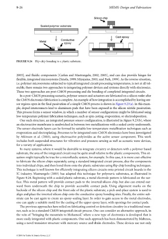
FIGURE 9.24 Flip-chip bonding to a plastic substrate.
2003], and fluidic components [Carlen and Mastrangelo, 2002, 2003], and can also provide hinges for
flexible, integrated microsystems [Smela, 1999; Miyajama, 2001; and Park, 1999]. As the reverse situation,
i.e. polymer microsystems subjected to typical integrated circuit processing temperatures, is not at all tol-
erable, there remain two approaches to integrating polymer devices and systems directly with electronics.
These two approaches are post-CMOS processing and die bonding of completed integrated circuits.
In a post-CMOS processing scenario, polymer sensors and actuators are fabricated on a silicon wafer after
the CMOS electronics fabrication is complete.An example of how integration is accomplished by leaving sen-
sor regions open in the final passivation of a simple CMOS process is shown in Figure 9.23(a).In this exam-
ple, doped interconnects lead to aluminum pads that have been exposed in the silicon nitride passivation.
This process forms a sensor window, in which a number of sensor configurations might be fabricated using
low-temperature polymer fabrication techniques, such as spin casting, evaporation, or electrodeposition.
One such structure, an integrated pressure sensor configuration, is illustrated in Figure 9.23(b), where
an electroactive membrane is sandwiched in between two metallizations with a sealed cavity underneath.
The sensor electrode layers can be formed by suitable low-temperature metallization techniques such as
evaporation and electroplating. Processes to be integrated onto CMOS electronics have been investigated
by Atkinson et al. (2003), using electroactive polyimides as the active sensor component. This work
includes both suspended structures for vibration and pressure sensing as well as acoustic wave devices,
for a variety of applications.
In many systems, where it would be desirable to integrate circuitry or detectors with a polymer based
substrate, the area of the integrated circuit may be quite small relative to the plastic components. This sit-
uation might typically be true for a microfluidic system, for example. In this case, it is more cost-effective
to fabricate the silicon chips separately, using a standard integrated circuit process, dice the components
into individual chips, and then bond them onto the plastic substrates using flip-chip bonding techniques.
This technique is well known for efficiently integrating silicon circuits onto printed circuit boards in the
IC industry. Mastrangelo (2003) has adapted this technique for polymeric substrates, as illustrated in
Figure 9.24. Beginning with a sealed plastic substrate, a metal electrode pattern is fabricated on the sur-
face. This metal pattern will provide contact pads to the inverted silicon chip, but also can extend out-
ward from underneath the chip to provide accessible contact pads. Using alignment marks on the
backside of the silicon chip and the front side of the plastic substrate, a pick-and-place system is used to
align and place the inverted silicon chip onto the conductive epoxy bonding sites. Finally, the entire sub-
strate can be cast again to create an epoxy-sealing layer. In order to gain access to the metal electrodes,
one can apply a suitable mold for the casting of the upper epoxy layer, with openings for contact pads.
The previous approaches have relied on fabricating control or detection circuitry in a traditional man-
ner, such as in a standard CMOS integrated circuit process. One can consider an alternative approach, in
the vein of “bringing the mountain to Mohamed,” where a new type of electronics is developed that is
more easily integrated with plastic components. One such approach has been demonstratedbyMaltezos,
using a novel transistor structure with mercury source and drain electrodes. These devices use not only
© 2006 by Taylor & Francis Group, LLC