
Page 506 -
P. 506
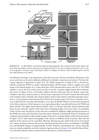
Polymer Microsystems: Materials and Fabrication                                            9-27


                                                    PDMS
                                   (a)                                  (c)
                                                        Reservoir


                                               Si/SiO
                                                     2


                                                       Ti/Au/Ti          Hg
                                                    Pentacene
                                   (b)


                           Source                             Drain


                          Gate


                                                      Transistor region           1000 µm

             FIGURE 9.25 (a) Microfluidic source/drain substrate being integrated onto oxidized, heavily doped silicon sub-
             strate with source/drain contacts and pentacene channel material, (b) top view of integrated structure, and (c) opti-
             cal micrographs of transistor region showing the ability to modulate the effective channel width using the mercury
             flow (after Maltezos et al. (2003)).


             microfluidic technology as an integral part of the electronics, but also the microfluidic fabrication of the
             source and drain can be used to fabricate additional microfluidic components and systems. The basic fab-
             rication approach is illustrated in Figure 9.25. The PDMS component of Figure 9.25(a) is formed ini-
             tially by a casting the PDMS in a master mold and peeling it off. The master mold is a negative-tone relief
             image of the desired pattern in a 15-µm-thick layer of the photosensitive epoxy resin SU-8. The PDMS
             solution is cast in the SU-8 mold, cured, and then removed. A separate, highly doped silicon substrate,
             also shown in Figure 9.25(a), is thermally oxidized and then patterned with two shadow mask steps.
             A shadow mask step is used to pattern an electron beam evaporation of Ti/Au/Ti contacts that will connect
             to the transistor source and drain,and a separate shadow mask is used to pattern a thermal evaporation of pen-
             tacene, a p-type polymer semiconductor that will form the transistor region of the device. Droplets of mer-
             cury are placed in the reservoirs and will adhere, even when the PDMS substrate is inverted for attachment
             to the silicon substrate. A brief exposure to an oxygen plasma allows a good bond between the PDMS and
             silicon dioxide. The highly doped silicon substrate will act as the gate electrode, and the thermal oxide
             forms the gate dielectric. Figure 9.25(b) shows the overlapping design of the device after it is assembled.
             In this current work, the mercury in the reservoirs is pumped by applying a slight mechanical pressure to
             the PDMS reservoirs, and it then flows down the narrow channels, contacting the Ti/Au/Ti electrodes and
             coming in close proximity in the transistor region of the device.A unique feature of these devices is shown
             in Figure 9.25(c), where optical micrographs of the mercury at different levels of pressure show that the
             position of the mercury can be controlled, effectively allowing the gate width of the device to be tuned.
             Low contact resistances between the mercury and the pentacene device layers are obtained ( 0.02MΩ-
             cm), and threshold voltages are approximately 18 Volts. Transistor characteristics for a device where the
             mercury extends completely across the transistor region are shown in Figure 9.26, where the linear behav-
             ior in the inset indicates ohmic contacts between the mercury and the pentacene.


             © 2006 by Taylor & Francis Group, LLC