
Page 503 -
P. 503
9-24 MEMS: Design and Fabrication
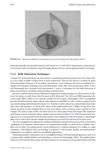
FIGURE 9.21 Aluminum mold plate and stamper for open mold casting (after Mastrangelo (2003)).
fabricated optically, but optically driven as well. Maruo et al. (1998, 2000) showed exotic, nanoscale spi-
ral structures, tubes and funnels using both single-photon and two-photon polymerization technology.
9.3.3 Bulk Fabrication Techniques
Compared to traditional metal and semiconductor machining materials, polymers have the unique abil-
ity to be readily available in liquid form at room temperature. This fact has allowed a number of useful
batch processing techniques to be developed, and extensive work in this area has been accomplished by a
number of researchers, including Carlen and Mastrangelo (2002, 2003) and Sundararajan (2004). Carlen
and Mastrangelo have developed and characterized a variety of techniques for the bulk fabrication of
plastic microsystems, including casting, bonding, and lamination.
In order to replicate plastic parts in bulk fashion using microcasting techniques, it is first necessary to fab-
ricate the stamp, or mold, from which the parts will be fabricated. The LIGA and DRIE approaches dis-
cussed earlier [Kim, 2000] are two methods suitable for this purpose. Mastrangelo (2003) accomplished
precisely this fabrication by using a silicon wafer patterned using DRIE, in order to form a stamper for the
open mold casting method depicted in Figure 9.21.The silicon wafer is placed in a recessed aluminum frame
and coated with parylene-C to aid the later release of the molded plastic part. ATeflon O-ring and an alu-
minum top plate are then clamped down on top of the silicon wafer, and epoxy resin is poured over the
stamper. The resin is cured at 80°C for three hours and is then peeled from the stamper. The aluminum
mold frames used to contain the silicon stamper wafer are shown in Figure 9.22.With the open-mold cast-
ing process, it is not guaranteed that the back surface of the molded part is flat. If necessary, a closed upper
plate can be used to form the part, simply necessitating an access hole for injection of the epoxy resin.
The most straightforward approach to sealing microfluidic channels and reservoirs from cast polymer
components is to laminate or bond them to an unpatterned coverfilm or substrate. For a flexible cover-
film, such as Mylar, the sealing process can be performed in a desktop laminator. For sealing to a rigid
coverplate, a thin adhesive layer and bonding is preferred. In this manner, flexible, patterned polymer
components can readily be sealed for microfluidic applications.
Laminating polymer components can be accomplished using a roll-type laminating process, such as in
acommercially available desktop unit from Kepro, as shownbyMastrangelo (2003). The molded plastic
substrate is first treated with acetone and then laminated to a transparent, 50-µm-thick Mylar cover film
© 2006 by Taylor & Francis Group, LLC