
Page 241 - Make Your Own PCBs with EAGLE from Schematic Designs to Finished Boards
P. 241
pins on a symbol and the pads on a package.
Symbols and packages are created independently and linked together by devices, allowing the
same package design to be used by a number of different symbols.
In Figure 11-3, the Part Editor is showing the device. This same editor window is also used when
you want to edit the symbol or one of the packages of the device. You will notice three new icons on
the toolbar to the right of the “Printer” icon that allow you to select the element of the device that you
want to edit.
Editing a Part
We need to fix the labels on this part because the anode and cathode of the colon and apostrophe of
the display are swapped over. You may be wondering if this is a change to the pad names or to the
symbol. Well, the pad names are just named 1 to 16 on both packages, so the change needs to be made
in the linkage between the pin names on the symbol and the pad names. This takes place for each
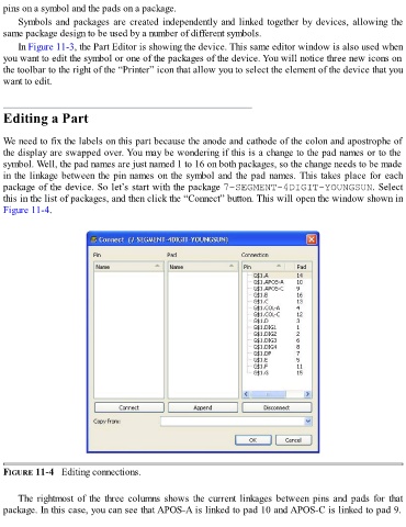
package of the device. So let’s start with the package 7-SEGMENT-4DIGIT-YOUNGSUN. Select
this in the list of packages, and then click the “Connect” button. This will open the window shown in
Figure 11-4.
FIGURE 11-4 Editing connections.
The rightmost of the three columns shows the current linkages between pins and pads for that
package. In this case, you can see that APOS-A is linked to pad 10 and APOS-C is linked to pad 9.