
Page 245 - Make Your Own PCBs with EAGLE from Schematic Designs to Finished Boards
P. 245
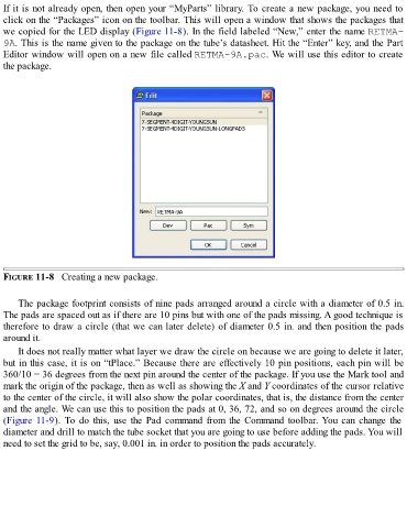
If it is not already open, then open your “MyParts” library. To create a new package, you need to
  click on the “Packages” icon on the toolbar. This will open a window that shows the packages that
  we copied for the LED display (Figure 11-8). In the field labeled “New,” enter the name RETMA-
  9A. This is the name given to the package on the tube’s datasheet. Hit the “Enter” key, and the Part

  Editor window will open on a new file called RETMA-9A.pac. We will use this editor to create
  the package.


  FIGURE 11-8   Creating a new package.


      The package footprint consists of nine pads arranged around a circle with a diameter of 0.5 in.
  The pads are spaced out as if there are 10 pins but with one of the pads missing. A good technique is
  therefore to draw a circle (that we can later delete) of diameter 0.5 in. and then position the pads

  around it.
      It does not really matter what layer we draw the circle on because we are going to delete it later,
  but in this case, it is on “tPlace.” Because there are effectively 10 pin positions, each pin will be

  360/10 = 36 degrees from the next pin around the center of the package. If you use the Mark tool and
  mark the origin of the package, then as well as showing the X and Y coordinates of the cursor relative
  to the center of the circle, it will also show the polar coordinates, that is, the distance from the center
  and the angle. We can use this to position the pads at 0, 36, 72, and so on degrees around the circle
  (Figure 11-9).  To  do  this,  use  the  Pad  command  from  the  Command  toolbar. You  can  change  the
  diameter and drill to match the tube socket that you are going to use before adding the pads. You will
  need to set the grid to be, say, 0.001 in. in order to position the pads accurately.