
Page 259 - Materials Chemistry, Second Edition
P. 259
246 4 Semiconductors
supplies sodium atoms with sufficient energy to promote an electron from the 3s
energy level into an empty 3p, or 4s orbital. The electron does not stay in the higher
energy level very long (typically ca.10 6 s) before it is spontaneously dropped to its
original ground state, releasing heat and/or light. There are three types of recombi-
[1]
nation :
(i) Band-to-band: an electron moves from the conduction band into an empty state
in the valence band associated with the hole. This yields a radiative emission,
whose wavelength is inversely proportional to the bandgap.
(ii) Trap-assisted: an electron falls into an energy level within the bandgap that is
associated with a dopant atom or structural defect.
(iii) Auger recombination: when a conduction-band electron and valence-band hole
recombine, rather than emitting light the energy may kick off an outer-shell
electron known as an Auger electron.
To understand the band structure and recombination process in more detail, we
must revisit some concepts of quantum physics discussed in Chapter 2. Recall that
matter and light exhibit both wave-and particle-like behavior. This duality may be
expressed by the de Broglie equation, which equates the wavelength and momen-
tum, p, of a particle (Eq. 2). The potential energy of an electron in a crystal lattice
depends on its location, and will be periodic due to the regular array of lattice atoms.
The periodic wave functions that result from solving the Schr€ odinger equation are
referred to as Bloch wave functions. Each wave function represents the energy of an
electron at a specific location in the lattice, referred to as k-space. Hence, an E-k
diagram may be constructed, with the potential energy of the electron on the y-axis,
and the wave vector, k, on the x-axis. The wave vector represents lattice directions of
the semiconductor crystal; changing values of k represents a change in momentum
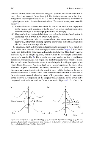
of the electron. A comparison of the simplified E-k diagrams for Si or Ge and a
compound semiconductor such as GaAs is shown in Figure 4.9. For GaAs, the
a b
E E
CB
E
c CB
Direct bandgap Photon
E
g
E
c
E
r
Phonon
E
v
VB E v
VB
-k k -k k
k vb k cb
Figure 4.9. Comparison of (a) direct bandgap (e.g., GaAs) and (b) indirect bandgap (e.g., Si, Ge)
materials. Reproduced with permission from Kasap, S. O. Principles of Electronic Materials and
Devices, 2nd ed., McGraw-Hill: New York, 2002.