
Page 262 - Materials Chemistry, Second Edition
P. 262
249
4.1. Properties and Types of Semiconductors
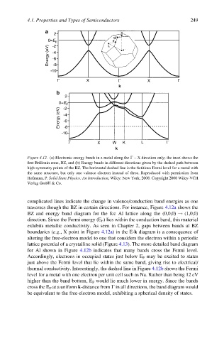
Figure 4.12. (a) Electronic energy bands in a metal along the G – X direction only; the inset shows the
first Brillouin zone, BZ, and (b) Energy bands in different directions given by the dashed path between
high-symmetry points of the BZ. The horizontal dashed line is the fictitious Fermi level for a metal with
the same structure, but only one valence electron instead of three. Reproduced with permission from
Hofmann, P. Solid State Physics: An Introduction, Wiley: New York, 2008. Copyright 2008 Wiley-VCH
Verlag GmbH & Co.
complicated lines indicate the change in valence/conduction band energies as one
traverses though the BZ in certain directions. For instance, Figure 4.12a shows the
BZ and energy band diagram for the fcc Al lattice along the (0,0,0) ! (1,0,0)
direction. Since the Fermi energy (E F ) lies within the conduction band, this material
exhibits metallic conductivity. As seen in Chapter 2, gaps between bands at BZ
boundaries (e.g., X point in Figure 4.12a) in the E-k diagram is a consequence of
altering the free-electron model to one that considers the electron within a periodic
lattice potential of a crystalline solid (Figure 4.13). The more detailed band diagram
for Al shown in Figure 4.12b indicates that many bands cross the Fermi level.
Accordingly, electrons in occupied states just below E F may be excited to states
just above the Fermi level that lie within the same band, giving rise to electrical/
thermal conductivity. Interestingly, the dashed line in Figure 4.12b shows the Fermi
level for a metal with one electron per unit cell such as Na. Rather than being 12 eV
higher than the band bottom, E F would lie much lower in energy. Since the bands
cross the E F at a uniform k-distance from G in all directions, the band diagram would
be equivalent to the free-electron model, exhibiting a spherical density of states.