
Page 266 - Materials Chemistry, Second Edition
P. 266
253
4.2. Silicon-Based Applications
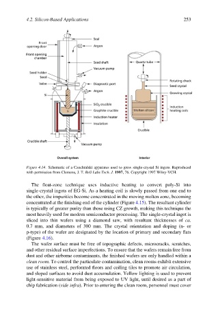
Figure 4.14. Schematic of a Czochralski apparatus used to grow single-crystal Si ingots. Reproduced
with permission from Clemens, J. T. Bell Labs Tech. J. 1997, 76. Copyright 1997 Wiley-VCH.
The float-zone technique uses inductive heating to convert poly-Si into
single-crystal ingots of EG-Si. As a heating coil is slowly passed from one end to
the other, the impurities become concentrated in the moving molten zone, becoming
concentrated at the finishing end of the cylinder (Figure 4.15). The resultant cylinder
is typically of greater purity than those using CZ growth, making this technique the
most heavily used for modern semiconductor processing. The single-crystal ingot is
sliced into thin wafers using a diamond saw, with resultant thicknesses of ca.
0.7 mm, and diameters of 300 mm. The crystal orientation and doping (n- or
p-type) of the wafer are designated by the location of primary and secondary flats
(Figure 4.16).
The wafer surface must be free of topographic defects, microcracks, scratches,
and other residual surface imperfections. To ensure that the wafers remain free from
dust and other airborne contaminants, the finished wafers are only handled within a
clean room. To control the particulate contamination, clean rooms exhibit extensive
use of stainless steel, perforated floors and ceiling tiles to promote air circulation,
and sloped surfaces to avoid dust accumulation. Yellow lighting is used to prevent
light-sensitive material from being exposed to UV light, until desired as a part of
chip fabrication (vide infra). Prior to entering the clean room, personnel must cover