
Page 131 - Mechanical Engineers Reference Book
P. 131
logical coding network which generates the appropriate digital
values to represent the state of the comparator outputs.
Regardless of the type of ADC used, the pin functions on
the integrated circuit are basically similar and generally com-
pr&e the power supply, the data bits, the start conversionin
I (SC or CONVERT) and the end of conversion pin (EOC or
‘f time
1. Conversion time: The conversion time is a measure of the
operating speed of the converter and is the time taken for
Figure 3.18 Integrator voltage variation
the complete translation of an analogue signal to digital
form. In many of the staircase and comparator and the
combination of standard voltages required to make up the integrating types of ADC this may be dependent on the
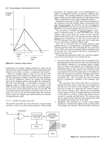
input value has been determined. The main components of the level of the analogue input signal. Faster conversion times
converter are a clock, a counter, a comparator and a DAC. are obtained with low-level inputs due to the manner in
When an analogue signal is input to the converter the which the conversion is completed. Successive approxima-
counter starts a count and passes a digital value to the DAC. tion and parallel conversion types of ADC have a fixed
The DAC generates a voltage to represent the most significant conversion time. This is because the same conversion
bit and the comparator assesses this against the analogue process is performed, regardless of the analogue input
input. If the analogue signal is greater than the voltage from level.
the DAC then the logic 1 in the MSB is retained. If the The conversion time of the ADC does not, however,
analogue signal is smaller then a logic 0 is assigned to the indicate the fastest rate at which data can be captured. If
MSB. This process is then repeated on the next most signifi- the data are to be stored in the computer’s RAM, then
cant bit and so on for all the other bits down to the LSB. The this must be done in a sequential and ordered manner.
conversion time for these types of converters may be of the This involves setting a base address and incrementing
order of 1@25 ps, but this will depend upon the hardware various registers to step the storage addresses of each byte
design. Figure 3.19 outlines the essential features of a success- of data placed in memory. Further time delays could be
ive approximation ADC. accrued in a sample and hold device. The minimum data
capture period is often therefore many times greater than
the specified conversion time of the ADC.
3.4.3.4 Parallel conversion type ADC 2. Resolution: The resolution of an ADC is the number
The parallel type ADC has by far the fastest conversion time employed to represent the digital output in binary form.
(at about 1 ps) but it is also the most expensive. With parallel For example, the resolution of an 8-bit ADC is limited to
Comparator
Digital
value
DAC
Figure 3.1 9 Successive-approximation ADC