
Page 127 - Mechanical Engineers Reference Book
P. 127
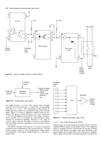
I     Inverter        T+5V                       +5 v
      3/10  Microprocessors, instrumentation and control


                           ..i,                                                      Load supply


                                    e
                                                           1
                                                          I


      Supply             Computer                                Darlington
                                                       r
      voltage            input                                     driver
                         signal
                                                            a
                                                           -


                                                                               Relay    Load
                                                                               supply
                                                                               voltage
                                                                               (+I 2 V)
       Figure 3.9  Output port digital interface for power switching


                        External
                        power
                                                      port
                                       Output to adjust:   7
                                        Motor speed,    0        *
                    Interface            Heater,
                                                        0
        output      hardware            Power valve,    0  -
                                                                 ).
                                        Position,       0  -                    Amplifier
                                        etc.
       Figure 3.10  Variable power output device                      DAC
                                                        0  -
                                                        0        *
       the  supply  voltage  is  common.  The  current  drawn  through   0   m            voltage
       each line, if it is connected, is 1,2,4 and 8 mA, corresponding
       with  bits  0,  1, 2  and  3.  The  summation  of  the  currents  at   0  -
       output therefore equates on a decimal to binary basis with the
       input. Figure  3.12 shows a  digital or switched  input  of  1011
       binary. This gives a current summation of  11 mA, equivalent   d   1
       to the corresponding decimal number. The output, a propor-
       tional  current,  can  be  converted  to  a  proportional  voltage   Figure 3.11  Variable power output using a DAC
       through  an  operational amplifier.  Because  of  the  range  of
       resistor  values  required, the  adder converter  is less popular   3.4.2.2  Pulse Width Modulation (PWM)
       than the ladder converter, which uses only two resistor values,
       i.e. R  and 2R.                                Output power from the interface  hardware  can be varied by
         The ladder converter  DAC (Figure 3.13) must be analysed   sending ON/OFF pulses to the power device.  The frequency
       using the network theorems of Thevenin and Norton. The end   range is normally between 2 and 10 kHz. If  the time ON and
       result is similar, however, with a proportional  voltage output   the time  OFF periods  are equal, then rapid  switching of  the
       corresponding  to the  digital  switched input  on  a  decimal-to-   power supply will transmit 50% of  the total power available.
       binary basis.                                  Due to the relatively high switching frequencies and the levels