
Page 123 - Mechanical Engineers Reference Book
P. 123
3/6 Microprocessors, instrumentation and control
r---li"""'i 8255PPI is the Intel 8253 chip, which provides three indepen-
Memory data bus
dent 16-bit counters, each with a count rate of up to 2.6 MHz.
The 8253 has various modes of operation but works basically
on the same principle as the timers in the 6522VIA.
3.2.4.5 Direct Memory Access (DMA)
In data-acquisition systems involving analogue and digital
signals suitably conditioned for inputting to a microcomputer
there is a limitation of about 100 kHz on the sampling rate
Figure 3.2 Port addressed I/O when using direct program control to transfer data to memory.
If it was necessary to acquire the maximum amount of data at
instructions of IN (or INP) and OUT in both low- and the highest speed, using the maximum amount of the compu-
high-level programming languages. ter's resources, then the DMA technique might be employed.
Although a number of I/O support chips are available, there This is a hardware technique which causes the micropro-
are essentially two which figure prominently with the memory cessor to momentarily abandon control of the system buses so
mapped and port addressed techniques. These are the 6522 that the DMA device can directly access the memory. The
versatile interface adapter, (VIA), usually associated with the DMA controller, connected to the I/O interface, needs to
memory mapped 6502 microprocessor systems and the 8255 know how many bytes are to be transferred and where in
programmable peripheral interface, (PPI), associated with memory the input data are to be stored. The data transfer rate
such processors as the 8080, 280 and 8086 in port addressed is much faster than in an interrupt servicing method and
systems. data-sampling rates of the order of 1 MHz are possible for
most microcomputers.
3.2.4.3 The 6522 VIA
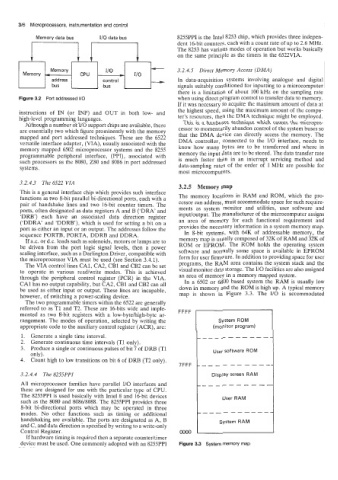
3.2.5 Memory map
This is a general interface chip which provides such interface
functions as two 8-bit parallel bi-directional ports, each with a The memory locations in RAM and ROM, which the pro-
pair of handshake lines and two 16-bit counter timers. The cessor can address, must accommodate space for such require-
ports, often designated as data registers A and B ('DRA' and ments as system monitor and utilities, user software and
'DRB') each have an associated data direction register input/output. The manufacturer of the microcomputer assigns
('DDRA' and 'DDRB'), which is used for setting a bit on a an area of memory for each functional requirement and
port as either an input or an output. The addresses follow the provides the necessary information in a system memory map.
sequence PORTB, PORTA, DDRB and DDRA. In 8-bit systems, with 64K of addressable memory, the
If ax. or d.c. loads such as solenoids, motors or lamps are to memory map is usually composed of 32K of RAM and 32K of
be driven from the port logic signal levels, then a power ROM or EPROM. The ROM holds the operating system
scaling interface, such as a Darlington Driver, compatible with software and normally some space is available in EPROM
the microprocessor VIA must be used (see Section 3.4.1). form for user firmware. In addition to providing space for user
The VIA control lines CA1, CA2, CB1 and CB2 can be set programs, the RAM area contains the system stack and the
to operate in various read/write modes. This is achieved visual monitor data storage. The 110 facilities are also assigned
through the peripheral control register (PCR) in the VIA. an area of memory in a memory mapped system.
CA1 has no output capability, but CA2, CB1 and CB2 can all In a 6502 or 6800 based system the RAM is usually low
be used as either input or output. These lines are incapable, down in memory and the ROM is high up. A typical memory
however, of switching a power-scaling device. map is shown in Figure 3.3. The I/O is accommodated
The two programmable timers within the 6522 are generally
referred to as T1 and T2. These are 16-bits wide and imple-
mented as two 8-bit registers with a low-byte/high-byte ar- FFFF
rangement. The modes of operation, selected by writing the System ROM
appropriate code to the auxiliary control register (ACR), are: (monitor program)
1. Generate a single time interval.
2. Generate continuous time intervals (T1 only).
3. Produce a single or continuous pulses of bit 7 of DRB (T1 User software ROM
only).
4. Count high to low transitions on bit 6 of DRB (T2 only).
7FFF
3.2.4.4 The 8255PPI
All microprocessor families have parallel 110 interfaces and
these are designed for use with the particular type of CPU.
The 8255PPI is used basically with Intel 8 and 16-bit devices
such as the 8080 and 8086/8088. The 8255PPI provides three User RAM
8-bit bi-directional ports which may be operated in three
modes. No other functions such as timing or additional
handshaking are available. The ports are designated as A, B
and C, and data direction is specified by writing to a write-only
Control Register. 0000
If hardware timing is required then a separate countedtimer
device must be used. One commonly adopted with an 8255PPI Figure 3.3 System memory map