
Page 56 - A Practical Guide from Design Planning to Manufacturing
P. 56
32 Chapter One
when the atoms of the crystal are pushed together. Depositing germa-
nium atoms, which are larger than silicon atoms, into the source and
drain tends to expand these areas. This pushes the atoms in the channel
closer together and improves hole mobility. Strained silicon is already
in use in the Intel 90-nm fabrication generation. 15
High-K Gate Dielectric. Gate oxide layers thinner than 1 nm are only a
few molecules thick and would have very large gate leakage currents.
Replacing the silicon dioxide, which is currently used in gate oxides, with
a higher permittivity material strengthens the electric field reaching the
channel. This allows for thicker gate oxides to provide the same control
of the channel at dramatically lower gate leakage currents.
Improved interconnects. Improvements in interconnect capacitance are
possible through further reductions in the permittivity of interlevel
dielectrics. However, improvements in resistance are probably not pos-
sible. Quasi-ideal interconnect scaling will rapidly reach aspect ratios
over 2, beyond which fabrication and cross talk noise with neighboring
wires become serious problems. The only element with less resistivity
than copper is silver, but it offers only a 10 percent improvement and
is very susceptible to electromigration. So, it seems unlikely that any
practical replacement for copper will be found, and yet at dimensions
below about 0.2 µm the resistivity of copper wires rapidly increases. 16
The density of free electrons and the average distance a free electron
travels before colliding with an atom determine the resistivity of a bulk
conductor. In wires whose dimensions approach the mean free path
length, the number of collisions is increased by the boundaries of the
wire itself. The poor scaling of interconnect delays may have to be
compensated for by scaling the upper levels of metal more slowly and
adding new metal layers more rapidly to continue to provide enough
L GATE
Gate oxide
Source Drain
Gate
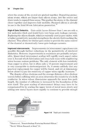
Figure 1-15 Triple gate transistor.
Current flow
15
Ghani et al., “Nanotechnology Featuring Strained-Silicon.”
16
David, “Silicon Research at Intel,” 21.