
Page 55 - A Practical Guide from Design Planning to Manufacturing
P. 55
The Evolution of the Microprocessor 31
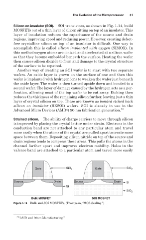
Silicon on insulator (SOI). SOI transistors, as shown in Fig. 1-14, build
MOSFETs out of a thin layer of silicon sitting on top of an insulator. This
layer of insulation reduces the capacitance of the source and drain
regions, improving speed and reducing power. However, creating defect-
free crystalline silicon on top of an insulator is difficult. One way to
accomplish this is called silicon implanted with oxygen (SIMOX). In
this method oxygen atoms are ionized and accelerated at a silicon wafer
so that they become embedded beneath the surface. Heating the wafer
then causes silicon dioxide to form and damage to the crystal structure
of the surface to be repaired.
Another way of creating an SOI wafer is to start with two separate
wafers. An oxide layer is grown on the surface of one and then this
wafer is implanted with hydrogen ions to weaken the wafer just beneath
the oxide layer. The wafer is then turned upside down and bonded to a
second wafer. The layer of damage caused by the hydrogen acts as a per-
foration, allowing most of the top wafer to be cut away. Etching then
reduces the thickness of the remaining silicon further, leaving just a thin
layer of crystal silicon on top. These are known as bonded etched back
silicon on insulator (BESOI) wafers. SOI is already in use in the
®
Advanced Micro Devices (AMD ) 90-nm fabrication generation. 14
Strained silicon. The ability of charge carriers to move through silicon
is improved by placing the crystal lattice under strain. Electrons in the
conduction band are not attached to any particular atom and travel
more easily when the atoms of the crystal are pulled apart to create more
space between them. Depositing silicon nitride on top of the source and
drain regions tends to compress these areas. This pulls the atoms in the
channel farther apart and improves electron mobility. Holes in the
valence band are attached to a particular atom and travel more easily
Gate SiO 2 Gate SiO 2
Source Drain Source Drain Si
Si
SiO 2
Bulk MOSFET SOI MOSFET
Figure 1-14 Bulk and SOI MOSFETs. (Thompson, “MOS Scaling.”)
14
“AMD and 90nm Manufacturing.”