
Page 52 - A Practical Guide from Design Planning to Manufacturing
P. 52
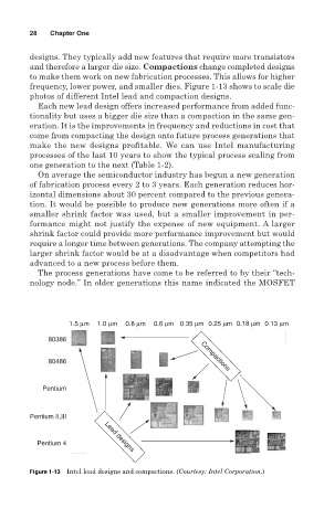
28   Chapter One

        designs. They typically add new features that require more transistors
        and therefore a larger die size. Compactions change completed designs
        to make them work on new fabrication processes. This allows for higher
        frequency, lower power, and smaller dies. Figure 1-13 shows to scale die
        photos of different Intel lead and compaction designs.
          Each new lead design offers increased performance from added func-
        tionality but uses a bigger die size than a compaction in the same gen-
        eration. It is the improvements in frequency and reductions in cost that
        come from compacting the design onto future process generations that
        make the new designs profitable. We can use Intel manufacturing
        processes of the last 10 years to show the typical process scaling from
        one generation to the next (Table 1-2).
          On average the semiconductor industry has begun a new generation
        of fabrication process every 2 to 3 years. Each generation reduces hor-
        izontal dimensions about 30 percent compared to the previous genera-
        tion. It would be possible to produce new generations more often if a
        smaller shrink factor was used, but a smaller improvement in per-
        formance might not justify the expense of new equipment. A larger
        shrink factor could provide more performance improvement but would
        require a longer time between generations. The company attempting the
        larger shrink factor would be at a disadvantage when competitors had
        advanced to a new process before them.
          The process generations have come to be referred to by their “tech-
        nology node.” In older generations this name indicated the MOSFET


                  1.5 µm  1.0 µm  0.8 µm  0.6 µm 0.35 µm 0.25 µm 0.18 µm 0.13 µm

             80386

             80486                                Compactions


           Pentium


        Pentium II,III


          Pentium 4        Lead designs


        Figure 1-13 Intel lead designs and compactions. (Courtesy: Intel Corporation.)