
Page 304 - Microsensors, MEMS and Smart Devices - Gardner Varadhan and Awadelkarim
P. 304
284 MICROSENSORS
Next, this reversible reaction is disturbed when the analyte molecule X reacts with the
chemisorbed oxygen species to release electrons and promulgate further reactions:
(8.51)
In a simple physical description, the tin oxide behaves like an n-type semiconductor and,
therefore, there is an increase in the electron carrier density n, and hence in the electrical
conductivity cr, of the material with increased gas concentration where
Aa = (8.52)
where /z n is the electron mobility.
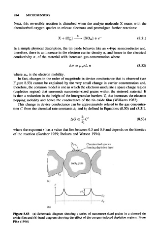
In fact, changes in the order of magnitude in device conductance that is observed (see
Figure 8.53) cannot be explained by the very small change in carrier concentration and,
therefore, the common model is one in which the electrons modulate a space charge region
(depletion region) that surrounds nanometer-sized grains within the sintered material. It
is then a reduction in the height of the intergranular barriers V s that increases the electron
hopping mobility and hence the conductance of the tin oxide film (Williams 1987).
This change in device conductance can be approximately related to the gas concentra-
tion C from the chemical rate constants k 1 and 2 defined in Equations (8.50) and (8.51).
AG oc -C r (8.53)
where the exponent r has a value that lies between 0.5 and 0.9 and depends on the kinetics
of the reaction (Gardner 1989; Ihokura and Watson 1994).
Chemisorbed species
forming depletion layer
Figure 8.53 (a) Schematic diagram showing a series of nanometre-sized grains in a sintered tin
oxide film and (b) band diagram showing the effect of the oxygen-induced depletion regions. From
Pike (1996)