
Page 307 - Microsensors, MEMS and Smart Devices - Gardner Varadhan and Awadelkarim
P. 307
BIO(CHEMICAL) SENSORS 287
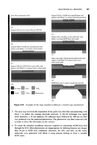
Figure 8.55 Example of the steps required to fabricate a resistive gas microsensor
5. The next step involved the deposition of the gold (Au) thin film and patterning with
Mask 3 to define the sensing electrode structure. A lift-off technique was again
used; therefore, a 10 nm titanium (Ti) adhesion layer followed by 300 nm Au film
was sputtered over the patterned photoresist. The photoresist was then removed with
acetone to leave the electrodes on the surface.
6. To create the ultrathin membrane structure required an anisotropic KOH back-etch
through the SCS. Most photoresists are inappropriate for defining features any deeper
than 20 urn in KOH etch conditions; therefore, the SiN x and SiO 2 on the wafer
underside were patterned with Mask 4 using plasma etching to form a suitable
KOH mask.