
Page 313 - Microsensors, MEMS and Smart Devices - Gardner Varadhan and Awadelkarim
P. 313
BIO(CHEMICAL) SENSORS 293
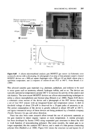
Figure 8.60 A silicon micromachined catalytic gate MOSFET gas sensor: (a) Schematic cross
section of a device with a silicon plug, (b) photograph of an array of four polymer-coated n -channel
MOSFET devices on a 1800 um square diaphragm with a 900 um (10 um thick) silicon plug to
equilibrate temperature, and (c) response of iridium (8 nm) FET at 140 °C. From Briand et al.
(2000)
This allowed catalytic gate materials (e.g. platinum, palladium, and iridium) to be used
to sense gases such as ammonia, ethanol, hydrogen sulfide, and so on. The devices are
typically operated at temperatures around 180 °C to increase the activity of the catalyst and
rate kinetics. The most recent MOSFET devices use silicon micromachining techniques to
define a silicon microplatform and thermal plug (Briand et al. 2000). Figure 8.60 shows
a schematic cross section of the device and a photograph of the FET device showing
a set of four FET sensors with an integrated heater and temperature sensor. A shift in
threshold voltage of about 220 mW is observed for a 20-ppm pulse of ammonia in air.
The power consumption of the device is greatly reduced to about 100 mW at 200 °C,
and again commercial arrays of these devices are being produced by a Swedish company
(Nordic Sensors) for gas and odour detection.
There has also been some research effort toward the use of polymeric materials as
the gate material to detect organic vapours at room temperature. A similar principle
has been developed by Janata (1992) using suspended gate structures to detect the shift
in work function of nonconducting polymers. But more recently, the metal gate is no
longer suspended, like the catalytic FET device, and is made of a thin porous conducting
polymer film (Hatfield et al. 2000). Figure 8.61 shows the structure (a) and layout (b) of