
Page 419 - Microsensors, MEMS and Smart Devices - Gardner Varadhan and Awadelkarim
P. 419
FABRICATION OF A MEMS-IDT ACCELEROMETER 399
the acceleration, the MEMS device can be used as an acceleration sensor. Alternatively,
the measurement can be done in the time domain, in which case the delay time of the
reflection from the reflectors is used to sense the acceleration.
14.3 FABRICATION OF A MEMS-IDT
ACCELEROMETER
We now illustrate the principles from the Worked Example 14.1 of a MEMS-IDT
accelerometer.
Worked Example E14.1: MEMS-IOT Accelerometer Objective:
There are three steps involved: First, a Rayleigh wave device consisting of an IDT on
a piezoelectric film is easily fabricated using conventional metal deposition or etching
techniques. These techniques are standard in integrated circuit (1C) processing and details
of SAW-IDT fabrication are provided in Chapter 12. Next, the reflector arrays can be
fabricated using silicon micromachining techniques. Finally, flip-chip bonding can be
used in order to reduce the handling of the substrate and hence maintain the performance
of the SAW substrate. The specific details are as follows (see Varadan et al.):
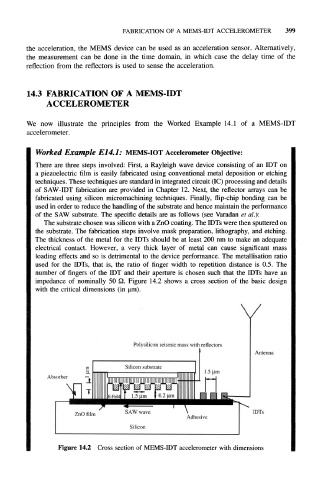
The substrate chosen was silicon with a ZnO coating. The IDTs were then sputtered on
the substrate. The fabrication steps involve mask preparation, lithography, and etching.
The thickness of the metal for the IDTs should be at least 200 nm to make an adequate
electrical contact. However, a very thick layer of metal can cause significant mass
loading effects and so is detrimental to the device performance. The metallisation ratio
used for the IDTs, that is, the ratio of finger width to repetition distance is 0.5. The
number of fingers of the IDT and their aperture is chosen such that the IDTs have an
impedance of nominally 50 £2. Figure 14.2 shows a cross section of the basic design
with the critical dimensions (in um).
Polysihcon seismic mass with reflectors
Antenna
Absorber
IDTs
Figure 14,2 Cross section of MEMS-IDT accelerometer with dimensions