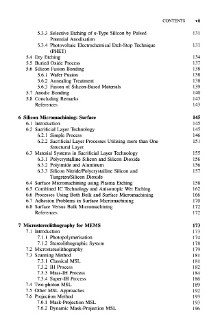
Page 8 - Microsensors, MEMS and Smart Devices - Gardner Varadhan and Awadelkarim
P. 8
CONTENTS     vii

           5.3.3  Selective  Etching of  n-Type  Silicon  by  Pulsed     131
                Potential  Anodisation
           5.3.4  Photovoltaic  Electrochemical  Etch-Stop  Technique    131
                (PHET)
      5.4  Dry  Etching                                                  134
      5.5  Buried Oxide  Process                                         137
      5.6  Silicon  Fusion  Bonding                                      138
           5.6.1  Wafer  Fusion                                          138
           5.6.2  Annealing  Treatment                                   138
           5.6.3  Fusion  of  Silicon-Based  Materials                   139
      5.7  Anodic Bonding                                                140
      5.8  Concluding Remarks                                            143
          References                                                     143

   6  Silicon  Micromachining:  Surface                                  145
      6.1  Introduction                                                  145
      6.2  Sacrificial  Layer  Technology                                145
           6.2.1  Simple  Process                                        146
           6.2.2  Sacrificial Layer  Processes  Utilising more  than  One  151
                Structural  Layer
      6.3  Material  Systems  in  Sacrificial Layer  Technology          155
           6.3.1  Polycrystalline  Silicon  and  Silicon  Dioxide        156
           6.3.2  Polyimide  and  Aluminum                               156
           6.3.3  Silicon  Nitride/Polycrystalline  Silicon  and         157
                Tungsten/Silicon  Dioxide
      6.4  Surface Micromachining  using Plasma  Etching                 158
      6.5  Combined  1C Technology  and  Anisotropic  Wet Etching        162
      6.6  Processes  Using Both  Bulk and  Surface Micromachining       166
      6.7  Adhesion  Problems  in  Surface Micromachining                170
      6.8  Surface  Versus Bulk  Micromachining                          172
          References                                                     172

   7  Microstereolithography for  MEMS                                   173
      7.1  Introduction                                                  173
           7.1.1  Photopolymerisation                                    174
           7.1.2  Stereolithographic  System                             178
      7.2  Microstereolithography                                        179
      7.3  Scanning Method                                               181
           7.3.1  Classical  MSL                                         181
           7.3.2  IH Process                                             182
           7.3.3  Mass-IH  Process                                       184
           7.3.4  Super-IH Process                                       186
      7.4  Two-photon  MSL                                               189
      7.5  Other  MSL  Approaches                                        192
      7.6  Projection  Method                                            193
           7.6.1  Mask-Projection  MSL                                   193
           7.6.2  Dynamic Mask-Projection  MSL                           196

