
Page 110 - Modern Control of DC-Based Power Systems
P. 110
74 Modern Control of DC-Based Power Systems
order to minimize the effect of spectral leakage, it is recommendable to
use windowing (e.g., Hanning) of the same length as the acquired signal.
Another practical aspect is the resolution of the digital to analog (D/A)
and analog to digital (A/D) converters to output the PRBS signal and
acquire the voltage and current measurements, respectively. Low resolutions
increase the minimum viable amplitude of the excitation. To get satisfac-
tory identification results, D/A and A/D converters are required to have
enough number of bits. For example, with 16-bit D/A and A/D converters
which give a resolution of 6:10mV on a voltage measurement of 6 200V
and a resolution of 0:31mV on the injected PRBS of 6 10V.
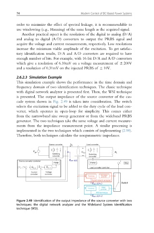
2.6.2.3 Simulation Example
This simulation example shows the performance in the time domain and
frequency domain of two identification techniques. The classic technique
with digital network analyzer is presented first. Then, the WSI technique
is presented. The output impedance of the source converter of the cas-
cade system shown in Fig. 2.49 is taken into consideration. The switch
selects the excitation signal to be added to the duty cycle of the load con-
verter, which operates in open-loop for simplicity. This comes either
from the narrowband sine sweep generator or from the wideband PRBS
generator. The two techniques take the same voltage and current measure-
ments from the impedance measurement point. A similar processing is
implemented in the two techniques which consists of implementing (2.98).
Therefore, both techniques calculate the nonparametric impedance.
Source converter I inj Load converter
+
V gs
V bus R L
Switching Switching
converter – converter
Z out_S(s)
Source converter controller +
PWM PWM Duty
V + G + G Load converter controller
ref C_V C_V
- –
Current Voltage
controller controller 1
Processing Sine sweep
generator
Digital network analyzer
Z out_S(jω k) Switch
PRBS
Processing
generator 2
WSI technique
Z out_S(jω k)
Figure 2.49 Identification of the output impedance of the source converter with two
techniques: the digital network analyzer and the Wideband System Identification
technique (WSI).