
Page 346 - Op Amps Design, Applications, and Troubleshooting
P. 346
324 SIGNAL PROCESSING CIRCUITS
integrator computes the area (height x width) of the input signal. This corre-
sponds to the mathematical operation in calculus called integration.
The integrator may also alter the shape of the input waveform. For example,
a square wave will be converted to a triangular wave in the process of being inte-
grated. When integrated, a triangle wave will produce a parabolic waveform that
very closely approximates a sinewave. In the case of a sinewave input, the output
will still be sinusoidal but may be shifted in phase and reduced in amplitude. For
sinewave inputs, the integrator acts as a simple low-pass filter.
7,6.1 Operation
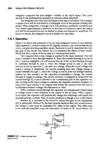
Figure 7,21 shows the schematic of an op amp integrator circuit. If you mentally
open capacitor Q (which is open for DC signals, anyway), you will see that the cir-
cuit is a simple inverting amplifier circuit. Resistors R 2 and RI determine the volt-
age gain of the circuit, and resistor R 3 is to minimize the effects of bias current.
Recall that the (-) input of the op amp is a virtual ground point.
Now suppose that a step voltage is applied to the input terminal. This will
cause a current to flow through resistor R^. Since the current flowing in or out of
the (-) input is negligible, we will assume that all of the current flowing through
an
RI continues through JR 2 d Q- Now, the voltage across R 2 and Q can only
increase as fast as capacitor Q can take on a charge. When the input voltage first
makes a change in amplitude, the current resulting from this voltage change is
routed entirely through Q. (Since the voltage across #2 does not change instantly,
neither can the current.) As the capacitor accumulates a charge, the current
through R 2 begins to change. The circuit, however, is designed to ensure that the
s
current through R 2 * never allowed to be a substantial part of the capacitor cur-
rent. As long as the input voltage is constant, the capacitor current is constant. As
long as the input returns to its original state before the capacitor has had time to
accumulate excessive voltage, this discussion is valid.
With a constant current through the capacitor, we will generate a linear ramp
of voltage across it (and therefore at the output of the op amp). With a square-
wave input, the capacitor will periodically charge and discharge with equal, but
opposite polarity, currents. This, of course, produces a triangle wave at the output.
Resistor R 2 is included in the circuit to reduce the gain at low frequencies
(DC in particular). Without JR 2, the bias currents (small as they are) would eventu-
ally charge Q and cause an undesired DC offset in the output. This offset may
even cause the amplifier to go into saturation. In terms of AC circuit theory, we
FIGURE 7.21 A basic op amp inte-
grator circuit.