Page 341 - Op Amps Design, Applications, and Troubleshooting
P. 341
Peak Detectors  319


        -VsATr since DI will be reverse-biased and the op amp will be operating with open-
        loop gain. On the positive alternation, the output may have to go as high as 5.7
         volts. That is, V PK of the input plus the forward drop of DI. Thus, the maximum
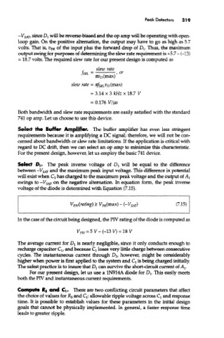
         output swing for purposes of determining the slew rate requirement is +5,7 - (-13)
         = 18.7 volts. The required slew rate for our present design is computed as


        Both bandwidth and slew rate requirements are easily satisfied with the standard
        741 op amp. Let us choose to use this device.

        Select the Buffer Amplifier. The buffer amplifier has even less stringent
        requirements because it is amplifying a DC signal; therefore, we will not be con-
        cerned about bandwidth or slew rate limitations. If the application is critical with
        regard to DC drift, then we can select an op amp to minimize this characteristic.
        For the present design, however, let us employ the basic 741 device.

        Select 0i« The peak inverse voltage of DI will be equal to the difference
        between -V SAT and the maximum peak input voltage. This difference in potential
        will exist when C\ has charged to the maximum peak voltage and the output of AI
        swings to -V SAT on the negative alternation. In equation form, the peak inverse
        voltage of the diode is determined with Equation (7.15).


        In the case of the circuit being designed, the PIV rating of the diode is computed as


        The average current for D! is nearly negligible, since it only conducts enough to
        recharge capacitor Q, and because Q loses very little charge between consecutive
        cycles. The instantaneous current through D lt however, might be considerably
        higher when power is first applied to the system and Q is being charged initially.
        The safest practice is to insure that DI can survive the short-circuit current of A^
             For our present design, let us use a 1N914A diode for D t. This easily meets
        both the PIV and instantaneous current requirements.

        Compute R 5 and Ci. There are two conflicting circuit parameters that affect
        the choice of values for R 5 and Q: allowable ripple voltage across Q and response
        time. It is possible to establish values for these parameters in the initial design
        goals mat cannot be physically implemented. In general, a faster response time
        leads to greater ripple.

