
Page 339 - Op Amps Design, Applications, and Troubleshooting
P. 339
Peak Detectors 317
tially isolates capacitor Q and leaves the charge trapped. The only discharge path
for Q is through RS and via leakage or op amp bias currents. In any case, the time
constant is much longer than the charge time constant, so Q holds its charge and
presents a steady input voltage to A 2 that is equal to the peak amplitude of the
input signal. A 2f of course, is simply a buffer amplifier and prevents unintentional
discharging of Q caused by loading from the following circuit.
Resistor R 5 is the primary discharge path for Q. If the input signal reduces its
average (Le., long-term) amplitude, then Q must be able to discharge to the new
peak level. If the R 5Ci time constant is too short, then the voltage on Q will not be
constant and will have a high value of ripple. On the other hand, if the R 5Ct time
constant is too long, then the circuit cannot respond quickly to changes in the
input amplitude. This characteristic is called fast attack (since Q responds quickly
to amplitude increases) and slow decay (since Q is slow to respond to signal
amplitude decreases).
Resistor R 3 limits the current into the (+) input of A 2 when power is discon-
nected from the circuit. Without this resistor, the input circuitry for A 2 may be
damaged as Q discharges through it. For capacitors smaller than 1 microfarad,
resistor R 3 can normally be omitted. Resistor R 4 is to minimize the effects of bias
currents in A 2. As in past circuits, we try to keep the resistance equal for both op
amp inputs.
Resistor R 2 limits the current into the (-) input of AI when power is removed
from the circuit. Again, this current comes from the discharge of Q. Resistor R l is
to minimize the effects of bias currents in AI and should be the same size as R 2,
7.5.2 Numerical Analysis
The basic numerical analysis of the dipper and buffer amplifier portions of the cir-
cuit (both voltage follower circuits) were presented in Chapter 2, and will not be
repeated here. Two additional characteristics that we want to analyze are
1, Lower frequency limit
2, Response time
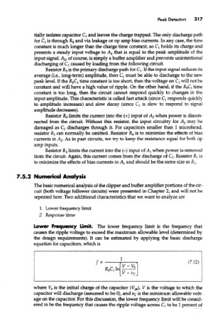
Lower Frequency Limit. The lower frequency limit is the frequency that
causes the ripple voltage to exceed the maximum allowable level (determined by
the design requirements). It can be estimated by applying the basic discharge
equation for capacitors, which is
where V G is the initial charge of the capacitor (V pk), V is the voltage to which the
capacitor will discharge (assumed to be 0), and v c is the minimum allowable volt-
age on the capacitor. For this discussion, the lower frequency limit will be consid-
ered to be the frequency that causes the ripple voltage across Q to be 1 percent of