Page 334 - Op Amps Design, Applications, and Troubleshooting
P. 334
312    SIGNAL PROCESSING CIRCUITS


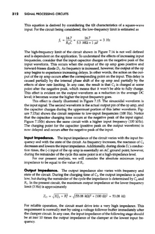
               This equation is derived by considering the tilt characteristics of a square-wave
               input. For the circuit being considered, the low-frequency limit is estimated as


               The high-frequency limit of the circuit shown in Figure 7.14 is not well defined
               and is dependent on the application. To understand the effects of increasing input
               frequencies, consider that the input capacitor charges on the negative peak of the
               input waveform. This occurs when the output of the op amp goes positive and
               forward-biases diode D\. As frequency is increased, however, the output of the op
               amp begins to experience increasing delays. In other words, the action on the out-
               put of the op amp occurs after the corresponding point on the input. This delay is
               caused partially by the internal phase shift of the op amp and partially by the
               effects of slew rate limiting. In any case, the result is that C 2 is charged at some
               point after the negative peak, which means that it won't be able to fully charge.
               This effect is evident on the output waveform as a reduction in the average IX
               level; it becomes worse the higher the input frequency goes.
                    This effect is clearly illustrated in Figure 7.15. The sinusoidal waveform is
               the input signal. The second waveform is the actual output pin of the op amp, and
               the capacitor charges during the uppermost portion of this latter waveform. Fig-
               ure 7.15(a) shows the circuit response to low-input frequencies (100 Hz). Notice
               that the capacitor charging time occurs at the negative peak of the input signal.
               Figure 7.15(b) shows the same circuit with a higher input frequency (100 kHz).
               The charging point for the capacitor (positive peak on the output waveform) is
               now delayed and occurs after the negative peak of the input.
               Input Impedance. The input impedance of the circuit varies with the input fre-

               quency and with the state of the circuit. As frequency increases, the reactance of C 2
               decreases and lowers the input impedance. Additionally, during diode Dj's conduc-
               tion times, the (-) input of the op amp is essentially an AC ground point; however,
               during the remainder of the cycle this same point is at a high-impedance level.
                    For our present analysis, we will consider the absolute minimum input
               impedance to be equal to the value of Rj.

               Output Impedance. The output impedance also varies with frequency and
               state of the circuit. During the charging time of C 2, the output impedance is quite
               low, but during the remainder of the cycle the impedance is determined by C 2 and
               R-I. In the present circuit, the maximum output impedance at the lower frequency
               limit (3 Hz) is approximately


               For reliable operation, the circuit must drive into a very high impedance. This
               requirement is normally met by using a voltage follower buffer immediately after
               the clamper circuit. In any case, the input impedance of the following stage should
               be at least 10 times the output impedance of the clamper at the lowest input fre-
               quency.

