
Page 329 - Op Amps Design, Applications, and Troubleshooting
P. 329
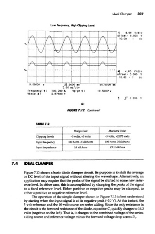
ideal Clamper  307


                               Low Frequency, High Clipping Level


                       TABLE 7.2
                                             Design Goal          Measured Value
                       Clipping levels     -3 volts, +3 volts  -3 volts, +2.875 volts
                       Input frequency    100 hertz-3 kilohertz  100 hertz-3 kilohertz
                       Input impedance       >8 kilohms           >9.1 kilohms


        7.4     (DIAL CLAMPER

                Figure 7.13 shows a basic diode clamper circuit. Its purpose is to shift the average
                or DC level of the input signal without altering the waveshape. Alternatively, an
                application may require that the peaks of the signal be shifted to some new refer-
                ence level. In either case, this is accomplished by clamping the peaks of the signal
                to a fixed reference level. Either positive or negative peaks may be clamped, to
                either a positive or negative reference level.
                    The operation of the simple clamper shown in Figure 7.13 is best understood
                by starting when the input signal is at its negative peak (-10 V). At this instant, the
                5-volt reference and the 10-volt source are series aiding. Since the only resistance in
                the circuit is the forward resistance of the diode, capacitor Q quickly charges to 14.3
                volts (negative on the left). That is, it charges to the combined voltage of the series-
                aiding source and reference voltage minus the forward voltage drop across D t.