
Page 330 - Op Amps Design, Applications, and Troubleshooting
P. 330
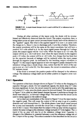
308    SIGNAL PROCESSING CIRCUITS


                  FIGURE 7.13 A simple biased clamper circuit is used to shift the DC or reference level of
                  the input signal.


                    During all other portions of the input cycle, the diode will be reverse-
               biased and effectively removed from the circuit. The output waveform, then, is
               being taken across an open circuit (reverse-biased diode) and will be identical to
               the "applied" signal. But what is the applied signal? It is now v I in series with
               the charge on Q. Since Q has no discharge path, it acts like a battery. Therefore,
               the output waveform will be the same as the input waveform, but will have a
               positive 14.3 volts added to it. As the input signal passes through its 0 voltage
               point, the output signal will be +14.3 volts. When the input is at +10 volts, the
               output will be at a +24.3-voit level. And when the input returns to the negative
               peak (-10 volts), the output will be at +4.3 volts. Any charge that has been lost
               on the capacitor because of leakage wiU be replaced when the input passes
               through its negative peak. As indicated by the resulting output waveform in
               Figure 7.13, the output signal appears to have its negative peaks clamped to the
               reference voltage (less a diode drop). Also, notice that the DC level of the out-
               put is now at +14.3 volts DC. For this reason, the circuit is sometimes called a
               DC restorer circuit.
                    If the diode is reversed, the positive peaks will be clamped to the reference
               voltage. The reference voltage itself can be either positive or negative (even vari-
               able).

        7.4.1 Operation
               The operation of the basic clamper shown in Figure 7.13 relies on the charging of a
               capacitor through a diode. For low-amplitude signals, the diode drop (0.7 volts)
               becomes significant. In fact, the circuit cannot be used at all if the peak input sig-
               nal is below 0.7 volts, since the diode cannot be forward-biased. The circuit shown
               in Figure 7.14 is called an ideal biased clamper because it performs as though the
               diode were ideal (i.e., no forward voltage drop). This means that the circuit can be
               used to clamp signals in the millivolt range.
                    Let us start our examination of the circuit in Figure 7.14 as the input reaches
               the negative peak. This will cause the output of the op amp to go in a positive
               direction and will forward-bias DI- The diode places a near short circuit around
               the op amp and essentially converts the circuit into a voltage follower with refer-
               ence to the (+) input. This means that the output of the op amp will be at approxi-
               mately the same voltage as the reference voltage (actually 0.7 volts higher). The (-)
               input of the op amp will also be at the reference voltage level. Capacitor C 2
               charges to the difference in potential between Vi and the reference voltage felt on
               the (-) input of the op amp. This action is similar to that described for the circuit in