
Page 331 - Op Amps Design, Applications, and Troubleshooting
P. 331
Ideal Clamper 309
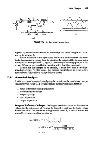
FIGURE 7.14 An ideal biased clamper circuit.
Figure 7.13, but notice the absence of a diode drop. The rate of charge for C 2 is lim-
ited by the value of RI-
For the remainder of the input cycle, the diode is reverse-biased. This effec-
tively disconnects the op amp from the circuit so the output will be the same as the
input plus the voltage across C 2. Again, C 2 has no rapid discharge path, so it will
act as a DC source and provide the damping action described previously.
In order for the clamper to be practical, it must drive into a very-high-
impedance circuit. For this reason, the damper circuit shown in Figure 7.14 is
nearly always followed by a voltage follower circuit.
7.4.2 Numerical Analysis
For the purpose of numerically analyzing the behavior of the ideal biased clamper
circuit shown in Figure 7.14, let us determine the following characteristics:
1. Range of reference voltage adjustment
2. Maximum input voltage
3. Frequency range
4. Input impedance
5. Output impedance
Range of Reference Voltage. Both upper and lower limits for the reference
voltage (at the wiper arm of F^ may be found by applying the basic voltage
divider equation. The minimum voltage occurs when Pj is moved toward the
minus 15-volt source and is computed as