
Page 336 - Op Amps Design, Applications, and Troubleshooting
P. 336
314 SIGNAL PROCESSING CIRCUITS
7.4.3 Practical Design Techniques
Let us now design an ideal biased-clamper circuit that performs according to the
following design goals:
1. Minimum input impedance 1.1 kilohms
2. Input voltage range 500 millivolts through 2 volts (peak)
3. Reference levels -1.0 volt through +2 volts
4. Minimum input frequency 20 hertz
Computation and selection of all components other than C 2 is similar to the meth-
ods described previously for the biased shunt clipper and will not be repeated
here. The value for capacitor C 2 can be determined by applying Equation (7.11).
where R x was computed in a preceding paragraph. We will use a standard 0.15-
microfarad capacitor for C 2.
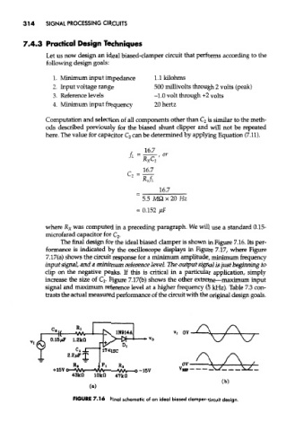
The final design for the ideal biased clamper is shown in Figure 7.16. Its per-
formance is indicated by the oscilloscope displays in Figure 7.17, where Figure
7.17(a) shows the circuit response for a mirumum amplitude, minimum frequency
input signal, and a minimum reference level. The output signal is just beginning to
clip on the negative peaks. If this is critical in a particular application, simply
increase the size of C 2. Figure 7.17(b) shows the other extreme—maximum input
signal and maximum reference level at a higher frequency (5 kHz). Table 7.3 con-
trasts the actual measured performance of the circuit with the original design goals.
FIGURE 7.16 Final schematic of an ideal biased clamper-circuit design.