Page 340 - Op Amps Design, Applications, and Troubleshooting
P. 340
318    SIGNAL PROCESSING CIRCUITS


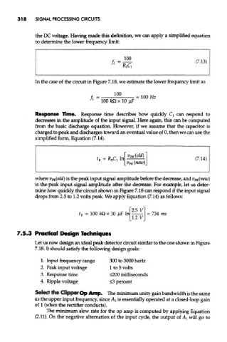
               the DC voltage. Having made this definition, we can apply a simplified equation
               to determine the lower frequency limit:


               In the case of the circuit in Figure 7.18, we estimate the lower frequency limit as


               Response Time. Response time describes how quickly Q can respond to
               decreases in the amplitude of the input signal. Here again, this can be computed
               from the basic discharge equation. However, if we assume that the capacitor is
               charged to peak and discharges toward an eventual value of 0, then we can use the
               simplified form, Equation (7.14).


               where v PK[old) is the peak input signal amplitude before the decrease, and v PK(new)
               is the peak input signal amplitude after the decrease. For example, let us deter-
               mine how quickly the circuit shown in Figure 7.18 can respond if the input signal
               drops from 2.5 to 1.2 volts peak. We apply Equation (7.14) as follows:


        7.5.3 Practical Design Techniques

               Let us now design an ideal peak detector circuit similar to the one shown in Figure
               7.18. It should satisfy the following design goals:

                  1. Input frequency range   300 to 3000 hertz
                 2. Peak input voltage       1 to 5 volts
                 3. Response time            <200 milliseconds
                 4. Ripple voltage           <3 percent

               Select the Clipper Op Amp. The minimum unity gain bandwidth is the same
               as the upper input frequency, since A x is essentially operated at a closed-loop gain
               of 1 (when the rectifier conducts).
                    The minimum slew rate for the op amp is computed by applying Equation
               (2.11). On the negative alternation of the input cycle, the output of A } will go to

