Page 332 - Op Amps Design, Applications, and Troubleshooting
P. 332
310    SIGNAL PROCESSING CIRCUITS


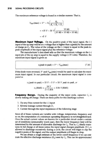
               The maximum reference voltage is found in a similar manner. That is,


               Maximum Input Voltage. On the positive peak of the input signal, the (~)
               input of the op amp will be at a voltage that is higher than u^peak) by the amount
               of charge on C 2. The value of the voltage on the (-) input is equal to the peak-to-
               peak amplitude of the input signal plus the reference voltage.
                    The manufacturer's data sheet tells us that the maximum voltage on the (-)
               input pin of the op amp is equal to the supply voltage (+15 volts). Therefore, the
               maximum input signal is given as


               If the diode were reversed, V~ and V R£F(min) would be used to calculate the maxi-
               mum input signal. In our particular circuit, the maximum input signal is com-
               puted as


               Frequency Range. During the majority of the input cycle, capacitor C 2 is
               slowly leaking off charge. There are three paths for this discharge current:

                 1. Op amp bias current for the (-) input
                 2. Reverse leakage current through Dj
                 3. Current through the input impedance of the following stage

               Since all of these currents are variable with voltage, temperature, frequency, and
               so on, the computation of a minimum operating frequency is not straightforward.
               Once the actual current values are known for a particular circuit under a certain
               set of conditions (presumably worst case), then the lower frequency limit will be
               determined by the amount of allowable discharge for C 2. That is, C 2 ideally main-
               tains its full charge at all times unless the input signal changes amplitude. If C 2 is
               allowed to discharge excessively during a cycle, the circuit will begin to clip the
               negative peaks of the signal, and the output amplitude will begin to drop.
                    We can obtain a rough estimate of the lower cutoff frequency if we can esti-
               mate the effective discharge resistance (R x) seen by C 2. This can be approximated

