
Page 282 - Optical Communications Essentials
P. 282
Optical Link Design
272 Chapter Sixteen
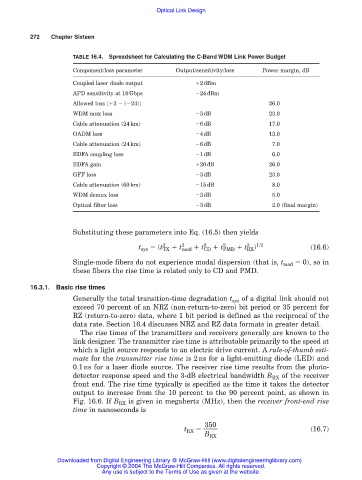
TABLE 16.4. Spreadsheet for Calculating the C-Band WDM Link Power Budget
Component/loss parameter Output/sensitivity/loss Power margin, dB
Coupled laser diode output 2dBm
APD sensitivity at 10Gbps 24dBm
Allowed loss [ 2 ( 24)] 26.0
WDM mux loss 3dB 23.0
Cable attenuation (24km) 6dB 17.0
OADM loss 4dB 13.0
Cable attenuation (24km) 6dB 7.0
EDFA coupling loss 1dB 6.0
EDFA gain 20dB 26.0
GFF loss 3dB 23.0
Cable attenuation (60km) 15dB 8.0
WDM demux loss 3dB 5.0
Optical filter loss 3dB 2.0 (final margin)
Substituting these parameters into Eq. (16.5) then yields
2
2
2
2
2
t sys (t TX t mod t CD t PMD t RX ) 1/2 (16.6)
Single-mode fibers do not experience modal dispersion (that is, t mod 0), so in
these fibers the rise time is related only to CD and PMD.
16.3.1. Basic rise times
Generally the total transition-time degradation t sys of a digital link should not
exceed 70 percent of an NRZ (non-return-to-zero) bit period or 35 percent for
RZ (return-to-zero) data, where 1 bit period is defined as the reciprocal of the
data rate. Section 16.4 discusses NRZ and RZ data formats in greater detail.
The rise times of the transmitters and receivers generally are known to the
link designer. The transmitter rise time is attributable primarily to the speed at
which a light source responds to an electric drive current. A rule-of-thumb esti-
mate for the transmitter rise time is 2ns for a light-emitting diode (LED) and
0.1ns for a laser diode source. The receiver rise time results from the photo-
detector response speed and the 3-dB electrical bandwidth B RX of the receiver
front end. The rise time typically is specified as the time it takes the detector
output to increase from the 10 percent to the 90 percent point, as shown in
Fig. 16.6. If B RX is given in megahertz (MHz), then the receiver front-end rise
time in nanoseconds is
350
t RX (16.7)
B RX
Downloaded from Digital Engineering Library @ McGraw-Hill (www.digitalengineeringlibrary.com)
Copyright © 2004 The McGraw-Hill Companies. All rights reserved.
Any use is subject to the Terms of Use as given at the website.